


In the search to create materials that can withstand extreme radiation, Yanwen Zhang, a researcher at the Department of Energy’s Oak Ridge National Laboratory, says that materials scientists must think outside the box.

ORNL welcomed six technology innovators to join the fourth cohort of Innovation Crossroads, the Southeast’s only entrepreneurial research and development program based at a U.S. Department of Energy national laboratory.
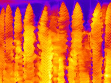
A team led by the Department of Energy’s Oak Ridge National Laboratory synthesized a tiny structure with high surface area and discovered how its unique architecture drives ions across interfaces to transport energy or information.

Matthew R. Ryder, a researcher at the Department of Energy’s Oak Ridge National Laboratory, has been named the 2020 Foresight Fellow in Molecular-Scale Engineering.

In the Physics Division of the Department of Energy’s Oak Ridge National Laboratory, James (“Mitch”) Allmond conducts experiments and uses theoretical models to advance our understanding of the structure of atomic nuclei, which are made of various combinations of protons and neutrons (nucleons).

As a teenager, Kat Royston had a lot of questions. Then an advanced-placement class in physics convinced her all the answers were out there.

Rigoberto “Gobet” Advincula has been named Governor’s Chair of Advanced and Nanostructured Materials at Oak Ridge National Laboratory and the University of Tennessee.

Liam Collins was drawn to study physics to understand “hidden things” and honed his expertise in microscopy so that he could bring them to light.
Scientists at have experimentally demonstrated a novel cryogenic, or low temperature, memory cell circuit design based on coupled arrays of Josephson junctions, a technology that may be faster and more energy efficient than existing memory devices.
Ancient Greeks imagined that everything in the natural world came from their goddess Physis; her name is the source of the word physics.