
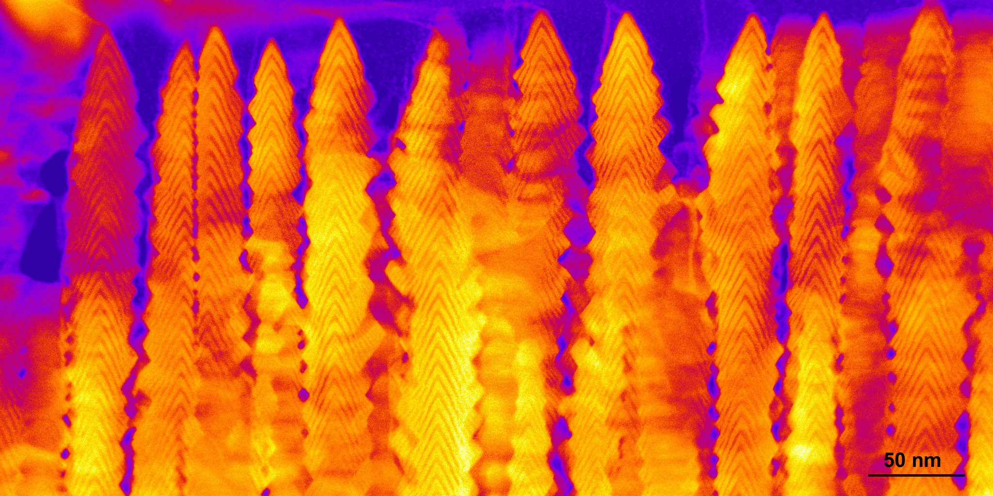
A nanobrush made by pulsed laser deposition of CeO2 and Y2O3 with dim and bright bands, respectively, is seen in cross-section with scanning transmission electron microscopy. Credit: Oak Ridge National Laboratory, U.S. Dept. of Energy
OAK RIDGE, Tenn., June 8, 2020 – A team led by the Department of Energy’s Oak Ridge National Laboratory synthesized a tiny structure with high surface area and discovered how its unique architecture drives ions across interfaces to transport energy or information. Their “nanobrush” contains bristles made of alternating crystal sheets with vertically aligned interfaces and plentiful pores.
“These are major technical accomplishments and may prove useful in advancing energy and information technologies,” said ORNL’s Ho Nyung Lee, who led the study published in Nature Communications. “This is an excellent example of work that is only feasible with the unique expertise and capabilities available at national labs.”
The team’s researchers hail from DOE national labs Oak Ridge and Argonne and Massachusetts Institute of Technology, or MIT, University of South Carolina, Columbia, and University of Tennessee, Knoxville.
The bristles of their multilayer crystal, or “supercrystal,” are grown freestanding on a substrate. Former ORNL postdoctoral fellow Dongkyu Lee synthesized the supercrystals using pulsed laser epitaxy to deposit and build up alternating layers of fluorite-structure cerium oxide (CeO2) and bixbyite-structure yttrium oxide (Y2O3). Realization of the nanoscale bristles was made possible by the development of a novel precision synthesis approach that controls atom diffusion and aggregation during the growth of thin-film materials. Using scanning transmission electron microscopy, or STEM, former ORNL postdoctoral fellow Xiang Gao was surprised to discover atomically precise crystalline interfaces within the bristles.
To see the distribution of CeO2 and Y2O3 within the nanobrush, ORNL’s Jonathan Poplawsky measured samples from the bristles using atom probe tomography, or APT, at the Center for Nanophase Materials Sciences, a DOE Office of Science User Facility at ORNL. “APT is the only technique available that is capable of probing the three-dimensional positions of atoms in a material with sub-nanometer resolution and 10 parts per million chemical sensitivity,” Poplawsky said. “APT clarifies the local distributions of atoms within a nanosized object and was an excellent platform for providing information about the 3D structure of the interface between the cerium oxide and yttrium oxide layers.”
For a 2017 paper, the ORNL-led researchers used epitaxy by pulsed laser deposition to precisely synthesize nanobrushes with bristles containing only one compound. For the 2020 paper, they used the same method to layer two compounds, CeO2 and Y2O3, fabricating the first hybrid bristles with interfaces between the two materials. Traditionally, interfaces are aligned laterally by layering different crystals in thin films, whereas in the novel nanobrushes when grown on a particular surface, interfaces are aligned vertically through surface energy minimization in bristles that are only 10 nanometers wide — about 10,000 times thinner than a human hair.
“This is a truly innovative way to build crystalline nanoarchitectures, providing unprecedented vertical interfaces that were never thought viable,” Ho Nyung Lee said. “You cannot achieve these perfect crystalline architectures from any other synthesis method.”
He added, “There are many ways to utilize interfaces, which is why 2000 Nobel Prize winner Herbert Kroemer said, ‘the interface is the device.’” Conventionally, depositing layers of thin film materials on substrates creates interfaces that are horizontally aligned, allowing ions or electrons to move along the substrate’s 2D plane. The ORNL-led achievement is proof of concept that it is possible to create vertically aligned interfaces through which electrons or ions can be transported out of the substrate’s plane. Moreover, architectures like the nanobrush could be combined with other nanoscale architectures to create devices for quantum technologies and sensing as well as energy storage.
The low-energy configuration of the fluorite structure caused the formation of unique chevron patterns, or inverted “V” shapes. A slight mismatch between different structures of fluorite and bixbyite crystal subunits causes mismatch of the electronic charges at their interfaces, causing oxygen atoms to vacate the fluorite side, which leads to the formation of functional defects. The spaces that are left behind can form interfacial oxygen ions and create an atomic-scale channel through which the ions can flow. “We are using the interfaces not only to artificially create oxygen ions, but also to guide ion movement in a more deliberate way,” Lee said.
With the help of ORNL’s Matthew Chisholm, Gao used STEM to uncover the atomic structure of the crystal and electron energy-loss spectroscopy to reveal chemical and electronic insights about the interface. “We observed that a quarter of oxygen atoms are lost at the interfaces,” said Chisholm. “We were also surprised by the chevron growth pattern. It was critical at the beginning to really understand how the interfaces form within the bristles.”
The nanobrush has a high porosity, and its architecture is advantageous for applications needing large surface area to maximize electronic and chemical interactions, such as sensors, membranes and electrodes. But how could the scientists determine the porosity of their material? Neutrons — neutral particles that pass through materials without destroying them — provided an excellent tool for characterizing porosity of the bulk material. The scientists used resources of the Spallation Neutron Source, a DOE Office of Science User Facility at ORNL, for extended Q-range small-angle neutron scattering that determined the upper limit of porosity to be 49%. “Quickly grown bristles can provide about 200 times as much surface area as a 2D thin film,” said ORNL co-author Michael Fitzsimmons.
He added, “What we learn may advance applications of neutron science in the process. Whereas thin films do not provide sufficient surface area for neutron spectroscopy studies, ORNL’s novel nanobrush architecture does, and could be a platform for learning more about interfacial materials when an even brighter neutron beam becomes available at SNS’s Second Target Station, which is a funded construction project.”
Theoretical calculations of the material system from the electronic and atomic level supported findings about oxygen-vacancy creation at the interfaces. MIT contributor Lixin Sun performed density functional theory calculations and molecular dynamics simulations under the direction of Bilge Yildiz.
“Our theoretical calculations revealed how this interface can accommodate a largely different chemistry at this type of unique interface compared to bulk materials,” said Yildiz. The MIT calculations predicted the energy needed to remove a neutral oxygen atom to form a vacancy close to the interface or in the middle of a cerium oxide layer. “In particular, we found that a large fraction of oxygen ions is removed at the interface without deteriorating the lattice structure.”
Lee said, “Indeed, these critical interfaces could form inside of nanobrush architectures, making them more promising than conventional thin films in many technological applications. Their much greater surface area and larger number of interfaces — potentially, thousands inside each bristle — may prove a game changer in future technologies in which the interface is the device.”
The title of the paper is “Colossal oxygen vacancy formation at a fluorite-bixbyite interface.”
The DOE Office of Science supported the research. The work used resources of the Center for Nanophase Materials Sciences and the Spallation Neutron Source, which are DOE Office of Science User Facilities at ORNL, as well as resources of the National Energy Research Scientific Computing Center and the Advanced Photon Source, DOE Office of Science User Facilities at Lawrence Berkeley National Laboratory and Argonne National Laboratory, respectively.
UT-Battelle manages ORNL for DOE’s Office of Science. The single largest supporter of basic research in the physical sciences in the United States, the Office of Science is working to address some of the most pressing challenges of our time. For more information, please visit https://www.energy.gov/science/ . — Dawn Levy
