
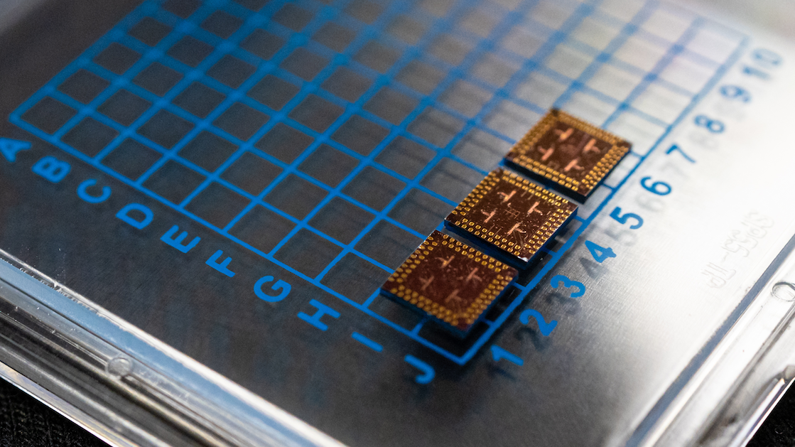
ORNL-developed cryogenic memory cell circuit designs fabricated onto these small chips by SeeQC, a superconducting technology company, successfully demonstrated read, write and reset memory functions. Credit: Carlos Jones/Oak Ridge National Laboratory, U.S. Dept. of Energy
Scientists at the Department of Energy’s Oak Ridge National Laboratory have experimentally demonstrated a novel cryogenic, or low temperature, memory cell circuit design based on coupled arrays of Josephson junctions, a technology that may be faster and more energy efficient than existing memory devices. If successfully scaled, this type of cryogenic memory array could advance a variety of applications including quantum and exascale computing.
“In our design, we have attempted a fundamentally different path that employs small, inductively coupled arrays of Josephson junctions,” said Yehuda Braiman of ORNL’s Computational Sciences and Engineering Division. “If scaled, such memory cell arrays could be orders of magnitude faster than existing memories while consuming very little power.”
The cells are designed to operate in super cold temperatures and were tested at just 4 Kelvin above absolute zero, about minus 452 degrees Fahrenheit. In conditions this cold, atoms slow down and certain materials lose resistance to the flow of electricity, becoming superconductors. Because superconductors have no resistance to electrical flow, they lose an almost negligible amount of energy as heat.
While the promise of building faster, more energy efficient computers based on these cryogenic technology principals has enticed researchers for decades, building reliable cryogenic “memories,” the parts of computers that store information for basic computing functions, has long remained an obstacle.
A different design
The ORNL-developed design deviates from existing cryogenic memory technologies because its memory cells, the localized parts of the circuit that hold one binary digit of a 0 or 1, known as one “bit” of information, are operated using three inductively coupled Josephson junctions.
Josephson junctions are well-established cryogenic electrical devices that can harness magnetic flux to store data. The ORNL design, which employs a small number of these junctions, could offer advantages over some of the recently studied low-temperature memory cells. Many of these technologies lean on a type of digital logic called single flux quantum, or SFQ. Others are based on magnetic Josephson junctions, which still pose some fabrication challenges for cryogenic memory applications.
“People are looking for something different,” Braiman said. “We are using typical junctions, which do not require any particular fabrication design. It’s an inherently different principle itself that makes the cell operate.”
Uniquely, their ternary design allows all of the basic memory operations — read, write and reset — to be implemented on the same three-Josephson-junction cell. This capability may help add stability while saving space and energy as the cell circuits are scaled into larger arrays, a step that has caused problems for existing technologies.
“The mechanism on which all of these [existing] types of cryogenic circuits are based is fundamentally unstable,” said Niketh Nair, a postdoctoral researcher at ORNL who worked on the design. “When you scale these circuits, the instability that exists in these systems may hit a critical point.”
Design confirmation
To confirm the viability of their new design, the ORNL team jointly tested the cell circuits with SeeQC, a superconducting technology company. SeeQC scientists fabricated the ORNL design onto 5 millimeter by 5 millimeter chips — about the diameter of a standard pencil eraser — with circuits at each corner.
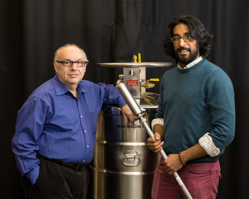
The chips were mounted onto a long pole, called a cryogenic probe, connected by wires to a desktop computer at room temperature. Scientists dunked the chips into a specialized container filled with liquid helium to cool the circuit to a temperature of 4 Kelvin. According to ORNL-directed test procedures, they then sent electrical pulses from the room temperature computer to test the memory function of the cells.
Tests of four cell circuit designs with slightly different specifications demonstrated not only that the cells work, but also that they function robustly and operate in a wider range of experimental parameters than the team had initially envisioned.
This confirmation comes three years after the ORNL team, which includes Braiman, Nair and Neena Imam, originally analyzed and simulated the logic of the cryogenic memory cell design in papers published in Superconductor Science and Technology and Physical Review E.
Though the researchers were excited to confirm their predictions, they are cautious to say their initial results will lead to a breakthrough. “What has been demonstrated is on a single cell level,” said Braiman. “What people care about are very large arrays of memory cells.”
As a next step, the ORNL team will work to implement their cells in increasingly large arrays and test designs using cryogenic testing equipment that the lab recently purchased. The new laboratory setup will enable future onsite research of cryogenic technologies.
Support for this work was provided by DOE’s Office of Science.
ORNL is managed by UT–Battelle for DOE’s Office of Science, the single largest supporter of basic research in the physical sciences in the United States. DOE’s Office of Science is working to address some of the most pressing challenges of our time. For more information, please visit energy.gov/science.