


Liam Collins was drawn to study physics to understand “hidden things” and honed his expertise in microscopy so that he could bring them to light.
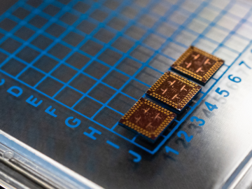
Scientists at have experimentally demonstrated a novel cryogenic, or low temperature, memory cell circuit design based on coupled arrays of Josephson junctions, a technology that may be faster and more energy efficient than existing memory devices.
Students often participate in internships and receive formal training in their chosen career fields during college, but some pursue professional development opportunities even earlier.
Ask Tyler Gerczak to find a negative in working at the Department of Energy’s Oak Ridge National Laboratory, and his only complaint is the summer weather. It is not as forgiving as the summers in Pulaski, Wisconsin, his hometown.
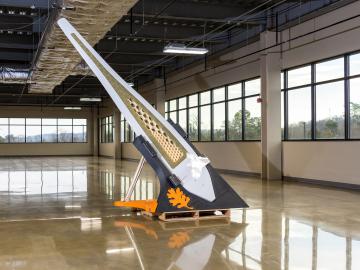
In the shifting landscape of global manufacturing, American ingenuity is once again giving U.S companies an edge with radical productivity improvements as a result of advanced materials and robotic systems developed at the Department of Energy’s Manufacturing Demonstration Facility (MDF) at Oak Ridge National Laboratory.
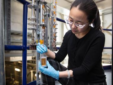
Researchers at the Department of Energy’s Oak Ridge National Laboratory, Pacific Northwest National Laboratory and Washington State University teamed up to investigate the complex dynamics of low-water liquids that challenge nuclear waste processing at federal cleanup sites.
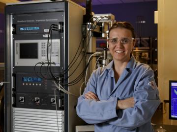
Vera Bocharova at the Department of Energy’s Oak Ridge National Laboratory investigates the structure and dynamics of soft materials—polymer nanocomposites, polymer electrolytes and biological macromolecules—to advance materials and technologies for energy, medicine and other applications.

Carbon fiber composites—lightweight and strong—are great structural materials for automobiles, aircraft and other transportation vehicles. They consist of a polymer matrix, such as epoxy, into which reinforcing carbon fibers have been embedded. Because of differences in the mecha...

Sergei Kalinin of the Department of Energy’s Oak Ridge National Laboratory knows that seeing something is not the same as understanding it. As director of ORNL’s Institute for Functional Imaging of Materials, he convenes experts in microscopy and computing to gain scientific insigh...

A new microscopy technique developed at the University of Illinois at Chicago allows researchers to visualize liquids at the nanoscale level — about 10 times more resolution than with traditional transmission electron microscopy — for the first time. By trapping minute amounts of...