
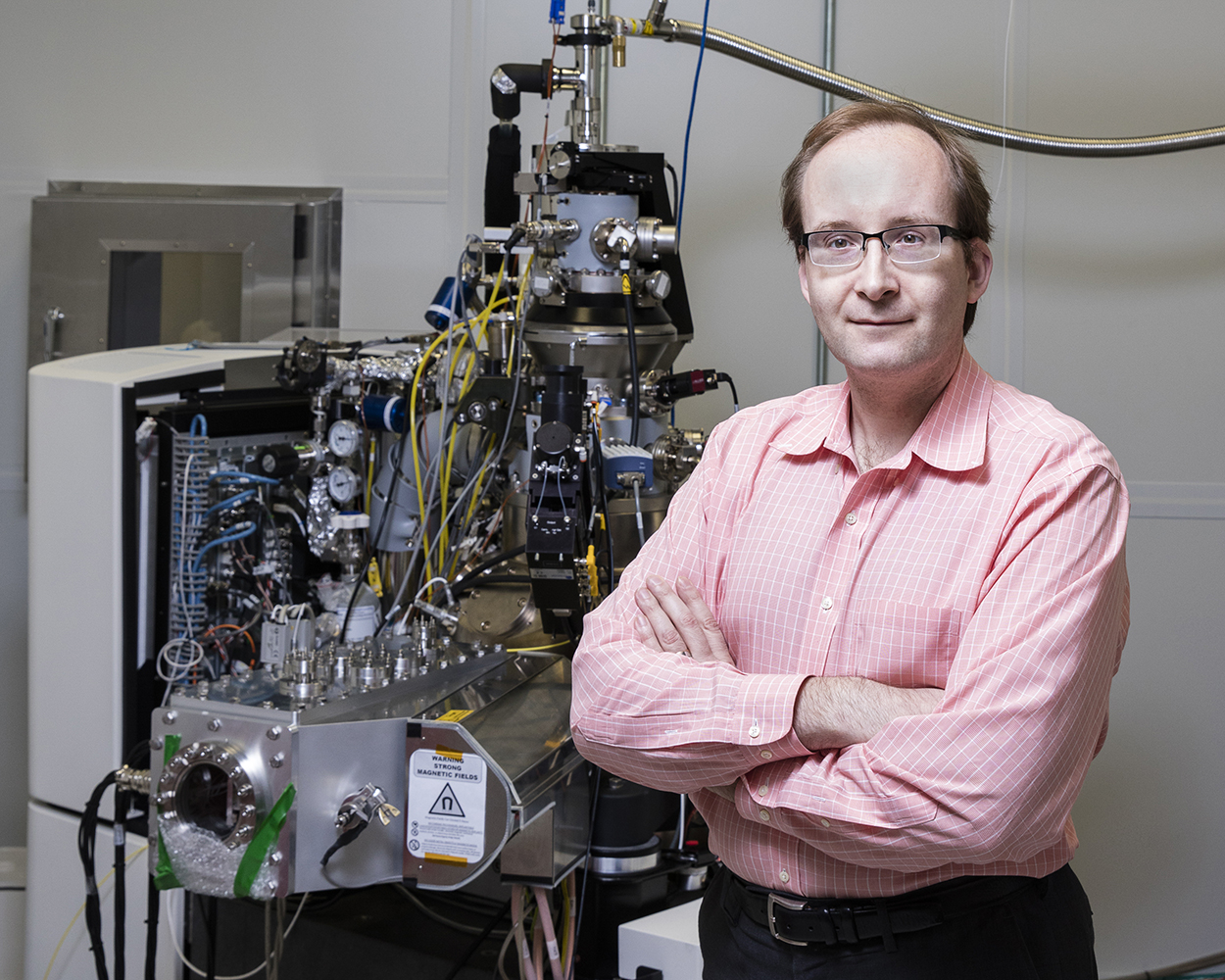
August 27, 2018 – Sergei Kalinin of the Department of Energy’s Oak Ridge National Laboratory knows that seeing something is not the same as understanding it. As director of ORNL’s Institute for Functional Imaging of Materials, he convenes experts in microscopy and computing to gain scientific insights that will inform the design of advanced materials for energy and information technologies.
“Knowing where each atom is in the solid is not the goal in itself,” Kalinin said. “It’s but a first step, from which we really want to understand the physical properties of a material.”
Kalinin is the author of approximately 570 papers, an inventor with at least 20 patents, and the winner of numerous awards, including a Presidential Early Career Award for Scientists and Engineers, the inaugural Medal for Scanning Probe Microscopy from the Royal Microscopical Society, and a Blavatnik National Award for Young Scientists.
Outside of his professional interests, he enjoys running and family time and is fond of Persian pop music star Leila Forouhar, German beer and TV’s The Big Bang Theory. At work, his attentions turn to smaller worlds with nanometer features that are 100,000 times thinner than a human hair.
At the Center for Nanophase Materials Sciences, a DOE Office of Science User Facility, Kalinin explores physical and chemical behaviors arising in synthetic nanostructures—some as small as a few atoms—that do not occur in larger structures.
His research focuses on three areas. The first is nanotechnology. Aiming to build materials from the bottom up, as Richard Feynman envisioned in 1959, Kalinin turns powerful imaging tools, such as electron and scanning probe microscopes, into what he calls “the atomic forge.” This endeavor to build quantum materials from scratch takes teamwork, such as from ORNL colleagues Stephen Jesse, who modifies electron microscopes and controls their beams to perform unusual tasks, and Bobby Sumpter, who incorporates theory and modeling to understand and predict material behavior. For a recent nanotechnology feat, Kalinin and collaborators used a scanning transmission electron microscope to place single dopant atoms in graphene.
Kalinin’s second concentration, machine learning, involves mining data from vast microscopy images and developing systemic ways to analyze it automatically. “When you have several hundred high-quality images per day or even per experiment, analysis becomes a bottleneck,” Kalinin said. “Human analytics cannot scale.” He works with Rick Archibald, Maxim Ziatdinov and other ORNL researchers to extract knowledge from atomically resolved images, identify phase transitions in materials, and recognize complex molecular assemblies on surfaces.
Kalinin’s third field is functional materials. He aims to understand populations of atoms that work together in functional domains to give materials useful properties, such as ferroelectricity (electric polarization that an applied electric field can reverse). With ORNL colleagues, he develops microscopes that can probe the electrochemistry of batteries and fuel cells (with Nina Balke) and the ferroelectricity of electronic materials (with Peter Maksymovych and Rama Vasudevan) and advances chemical imaging tools for materials analysis (with Olga Ovchinnikova). He often collaborates with a group headed by Anna Morozovska in Ukraine as well, developing theoretical frameworks to map ion diffusion in a lithium-ion battery cathode, measure oxygen-related reactions, and image energy distribution in ferroelectric materials.
From dacha to discovery
Kalinin became interested in science around age 10 at his family’s summer home outside Moscow, where he chanced upon his aunt’s high school chemistry textbooks. “The combination of boredom and curiosity is a remarkably good stimulus for studies, so I started to read them,” Kalinin recalled. “The country house is also a great place for doing ‘applied chemistry,’ such as fermentation and rapid burning experiments. After that I was seriously interested in chemistry.”
During high school, he took advanced placement classes and competed in the International Chemistry Olympiads, where his theory work ranked second, exempting him from high-school exams and guaranteeing his admission into any university in Russia.
He chose Moscow State University, which had a rigorous materials science program combining chemistry, physics and mathematics and requiring that students from their freshman year conduct original research and present their results at conferences. He also visited POSTECH, a university in Korea, intending to learn atomic force microscopy. However, the lab had not been set up before he arrived, so he mostly read scientific literature and became fascinated with techniques for imaging matter on the atomic level.
By the time he earned his master’s degree, Kalinin had amassed approximately 25 peer-reviewed publications. Entering the University of Pennsylvania in 1998, Kalinin investigated oxide materials using scanning probe microscopes and produced 30 more publications before getting his doctorate.
Accepting a Wigner postdoctoral fellowship in 2002, Kalinin came to ORNL and continued atomic imaging of oxides to understand their physics. He spent several years developing with Art Baddorf a massive system for pulsed laser deposition to synthesize advanced materials for studies.
Pursuing his interest in understanding and controlling matter on the atomic level, Kalinin began collaborating with ORNL’s electron microscopy group. Concurrently, he pursued two lines of inquiry. First, what science can be learned from an atomically resolved image of a material? Second, if the electron beam moves surface atoms as it images a material (a problem called “beam damage”), can scientists learn how to turn the problem into an asset by making the beam move atoms to specific locations?
“ORNL is lucky to have people like Stephen Jesse who know how to modify commercial tools with custom electronics, Andy Lupini and Mark Oxley who specialize in development of electronic microscopy optics and control systems and nanoscale measurements, and Rama Vasudevan and Maxim Ziatdinov who made a leap from physics into artificial intelligence,” said Kalinin. “The combination of this talent in one place, as well as close proximity to Titan and Summit [supercomputers] and the many talented scientists in the field of high-performance computing, allowed us to start doing four years ago what people worldwide are starting to do only now.”
Namely, researchers can now take control of the microscope’s electron beam, capture streaming video of the images, and respond based on computer analysis of the data.
“We are in a remarkable inflection point in science due to the merging of two enabling technologies—electron microscopy and artificial intelligence,” Kalinin said.
“Design of new materials for advanced energy and computing technologies is predicated on understanding material functionality on the atomic level and moving atoms where we need them to be. These opportunities are now within our grasp.”
The DOE Office of Science supports Kalinin’s research.
UT-Battelle manages ORNL for DOE’s Office of Science. The single largest supporter of basic research in the physical sciences in the United States, the Office of Science is working to address some of the most pressing challenges of our time. For more information, please visit www.energy.gov/science. –Dawn Levy
