An ORNL team used a simple process to implant atoms precisely into the top layers of ultra-thin crystals, yielding two-sided structures with different chemical compositions.

In the search to create materials that can withstand extreme radiation, Yanwen Zhang, a researcher at the Department of Energy’s Oak Ridge National Laboratory, says that materials scientists must think outside the box.

Juergen Rapp, a distinguished R&D staff scientist in ORNL’s Fusion Energy Division in the Nuclear Science and Engineering Directorate, has been named a fellow of the American Nuclear Society
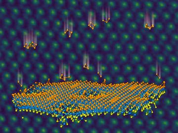
A team led by the Department of Energy’s Oak Ridge National Laboratory synthesized a tiny structure with high surface area and discovered how its unique architecture drives ions across interfaces to transport energy or information.

As a teenager, Kat Royston had a lot of questions. Then an advanced-placement class in physics convinced her all the answers were out there.

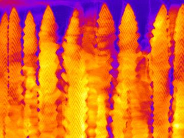
OAK RIDGE, Tenn., Feb. 27, 2020 — Researchers at Oak Ridge National Laboratory and the University of Tennessee achieved a rare look at the inner workings of polymer self-assembly at an oil-water interface to advance materials for neuromorphic computing and bio-inspired technologies.

An international team of researchers has discovered the hydrogen atoms in a metal hydride material are much more tightly spaced than had been predicted for decades — a feature that could possibly facilitate superconductivity at or near room temperature and pressure.

Rigoberto “Gobet” Advincula has been named Governor’s Chair of Advanced and Nanostructured Materials at Oak Ridge National Laboratory and the University of Tennessee.

Liam Collins was drawn to study physics to understand “hidden things” and honed his expertise in microscopy so that he could bring them to light.

Kathy McCarthy has been named director of the US ITER Project Office at the Department of Energy’s Oak Ridge National Laboratory, effective March 2020.