
Filter News
Area of Research
- Advanced Manufacturing (8)
- Biology and Environment (32)
- Building Technologies (2)
- Clean Energy (74)
- Computational Engineering (1)
- Computer Science (7)
- Energy Sciences (1)
- Fuel Cycle Science and Technology (1)
- Fusion and Fission (16)
- Fusion Energy (9)
- Isotope Development and Production (1)
- Isotopes (2)
- Materials (37)
- Materials for Computing (8)
- National Security (17)
- Neutron Science (7)
- Nuclear Science and Technology (22)
- Nuclear Systems Modeling, Simulation and Validation (2)
- Sensors and Controls (1)
- Supercomputing (25)
News Type
News Topics
- (-) Advanced Reactors (25)
- (-) Artificial Intelligence (46)
- (-) Machine Learning (28)
- (-) Microscopy (36)
- (-) Nuclear Energy (58)
- (-) Security (18)
- (-) Sustainable Energy (88)
- 3-D Printing/Advanced Manufacturing (87)
- Big Data (30)
- Bioenergy (56)
- Biology (60)
- Biomedical (36)
- Biotechnology (14)
- Buildings (41)
- Chemical Sciences (47)
- Clean Water (20)
- Climate Change (59)
- Composites (20)
- Computer Science (109)
- Coronavirus (34)
- Critical Materials (24)
- Cybersecurity (26)
- Decarbonization (42)
- Education (3)
- Element Discovery (1)
- Energy Storage (86)
- Environment (116)
- Exascale Computing (13)
- Fossil Energy (1)
- Frontier (18)
- Fusion (30)
- Grid (42)
- High-Performance Computing (46)
- Hydropower (8)
- Irradiation (2)
- Isotopes (32)
- ITER (6)
- Materials (101)
- Materials Science (95)
- Mathematics (5)
- Mercury (9)
- Molten Salt (7)
- Nanotechnology (44)
- National Security (36)
- Net Zero (6)
- Neutron Science (84)
- Partnerships (28)
- Physics (44)
- Polymers (26)
- Quantum Computing (14)
- Quantum Science (38)
- Renewable Energy (1)
- Simulation (19)
- Space Exploration (13)
- Statistics (3)
- Summit (28)
- Transformational Challenge Reactor (4)
- Transportation (72)
Media Contacts
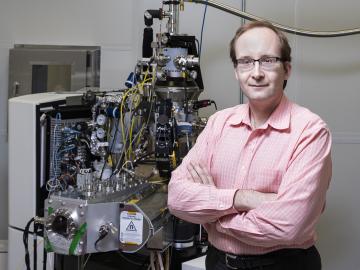
Sergei Kalinin of the Department of Energy’s Oak Ridge National Laboratory knows that seeing something is not the same as understanding it. As director of ORNL’s Institute for Functional Imaging of Materials, he convenes experts in microscopy and computing to gain scientific insigh...
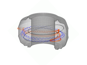
Fusion scientists from Oak Ridge National Laboratory are studying the behavior of high-energy electrons when the plasma that generates nuclear fusion energy suddenly cools during a magnetic disruption. Fusion energy is created when hydrogen isotopes are heated to millions of degrees...
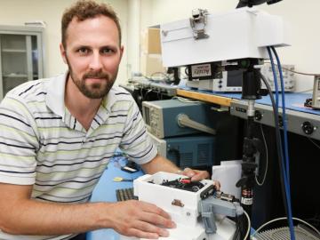
As leader of the RF, Communications, and Cyber-Physical Security Group at Oak Ridge National Laboratory, Kerekes heads an accelerated lab-directed research program to build virtual models of critical infrastructure systems like the power grid that can be used to develop ways to detect and repel cyber-intrusion and to make the network resilient when disruption occurs.

Brixon, Inc., has exclusively licensed a multiparameter sensor technology from the Department of Energy’s Oak Ridge National Laboratory. The integrated platform uses various sensors that measure physical and environmental parameters and respond to standard security applications.

A shield assembly that protects an instrument measuring ion and electron fluxes for a NASA mission to touch the Sun was tested in extreme experimental environments at Oak Ridge National Laboratory—and passed with flying colors. Components aboard Parker Solar Probe, which will endure th...
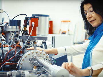
It may take a village to raise a child, according to the old proverb, but it takes an entire team of highly trained scientists and engineers to install and operate a state-of-the-art, exceptionally complex ion microprobe. Just ask Julie Smith, a nuclear security scientist at the Depa...
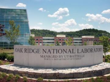
James Peery, who led critical national security programs at Sandia National Laboratories and held multiple leadership positions at Los Alamos National Laboratory before arriving at the Department of Energy’s Oak Ridge National Laboratory last year, has been named a...
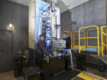
A scientific team led by the Department of Energy’s Oak Ridge National Laboratory has found a new way to take the local temperature of a material from an area about a billionth of a meter wide, or approximately 100,000 times thinner than a human hair. This discove...
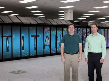
A team of researchers from the Department of Energy’s Oak Ridge National Laboratory has married artificial intelligence and high-performance computing to achieve a peak speed of 20 petaflops in the generation and training of deep learning networks on the

Material surfaces and interfaces may appear flat and void of texture to the naked eye, but a view from the nanoscale reveals an intricate tapestry of atomic patterns that control the reactions between the material and its environment. Electron microscopy allows researchers to probe...


