


Juergen Rapp, a distinguished R&D staff scientist in ORNL’s Fusion Energy Division in the Nuclear Science and Engineering Directorate, has been named a fellow of the American Nuclear Society
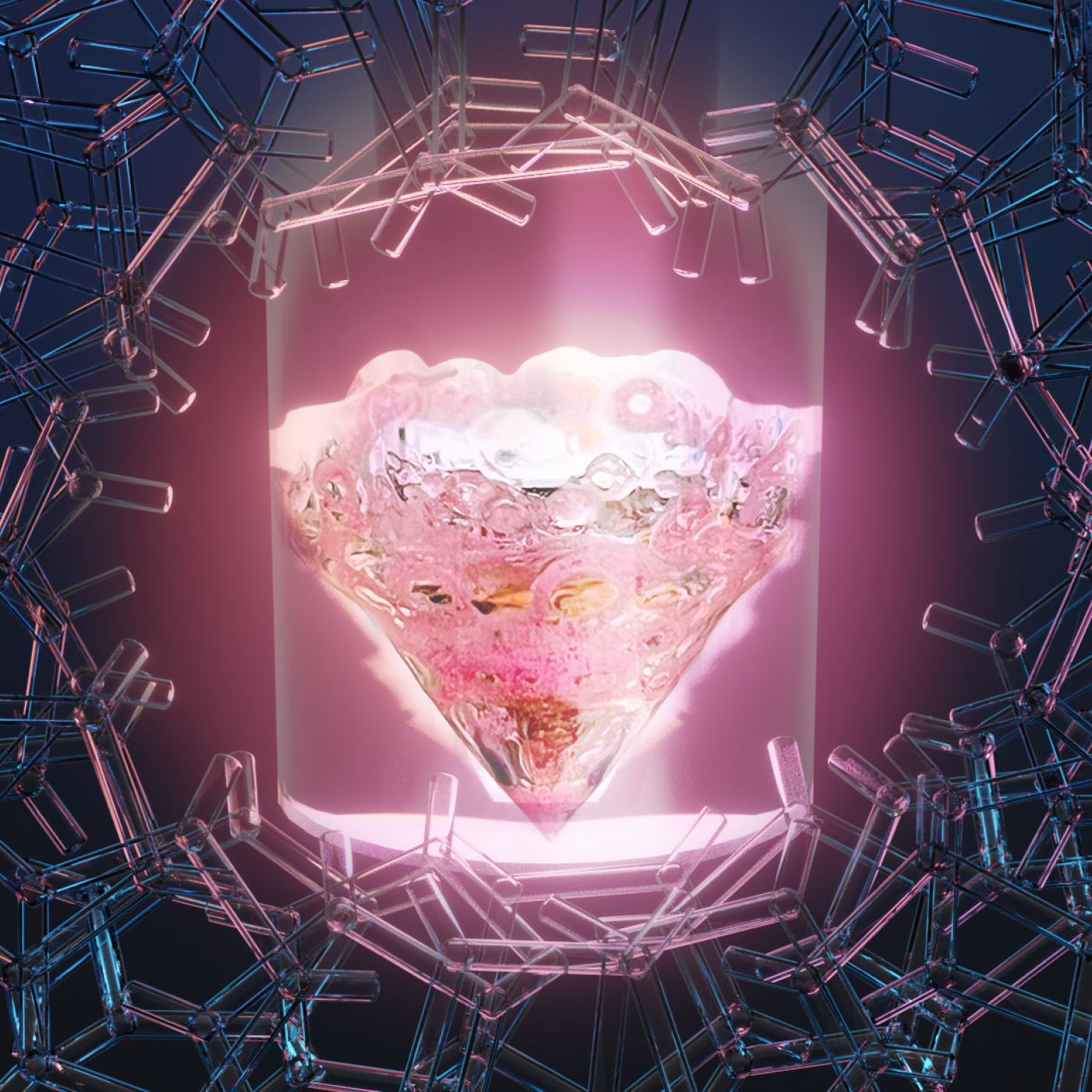
A team led by the Department of Energy’s Oak Ridge National Laboratory synthesized a tiny structure with high surface area and discovered how its unique architecture drives ions across interfaces to transport energy or information.

As a teenager, Kat Royston had a lot of questions. Then an advanced-placement class in physics convinced her all the answers were out there.

Rigoberto “Gobet” Advincula has been named Governor’s Chair of Advanced and Nanostructured Materials at Oak Ridge National Laboratory and the University of Tennessee.

Liam Collins was drawn to study physics to understand “hidden things” and honed his expertise in microscopy so that he could bring them to light.