


The INFUSE fusion program announced a second round of 2020 public-private partnership awards to accelerate fusion energy development.

Chuck Kessel was still in high school when he saw a scientist hold up a tiny vial of water and say, “This could fuel a house for a whole year.”
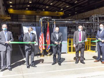
Department of Energy Under Secretary for Science Paul Dabbar joined Oak Ridge National Laboratory leaders for a ribbon-cutting ceremony to mark progress toward a next-generation fusion materials project.
From materials science and earth system modeling to quantum information science and cybersecurity, experts in many fields run simulations and conduct experiments to collect the abundance of data necessary for scientific progress.
Oak Ridge National Laboratory researchers have built a novel microscope that provides a “chemical lens” for viewing biological systems including cell membranes and biofilms.

Research by an international team led by Duke University and the Department of Energy’s Oak Ridge National Laboratory scientists could speed the way to safer rechargeable batteries for consumer electronics such as laptops and cellphones.

In the race to identify solutions to the COVID-19 pandemic, researchers at the Department of Energy’s Oak Ridge National Laboratory are joining the fight by applying expertise in computational science, advanced manufacturing, data science and neutron science.

Scientists at Oak Ridge National Laboratory used a focused beam of electrons to stitch platinum-silicon molecules into graphene, marking the first deliberate insertion of artificial molecules into a graphene host matrix.

Liam Collins was drawn to study physics to understand “hidden things” and honed his expertise in microscopy so that he could bring them to light.
Scientists at have experimentally demonstrated a novel cryogenic, or low temperature, memory cell circuit design based on coupled arrays of Josephson junctions, a technology that may be faster and more energy efficient than existing memory devices.