

An ORNL team used a simple process to implant atoms precisely into the top layers of ultra-thin crystals, yielding two-sided structures with different chemical compositions.

In the search to create materials that can withstand extreme radiation, Yanwen Zhang, a researcher at the Department of Energy’s Oak Ridge National Laboratory, says that materials scientists must think outside the box.
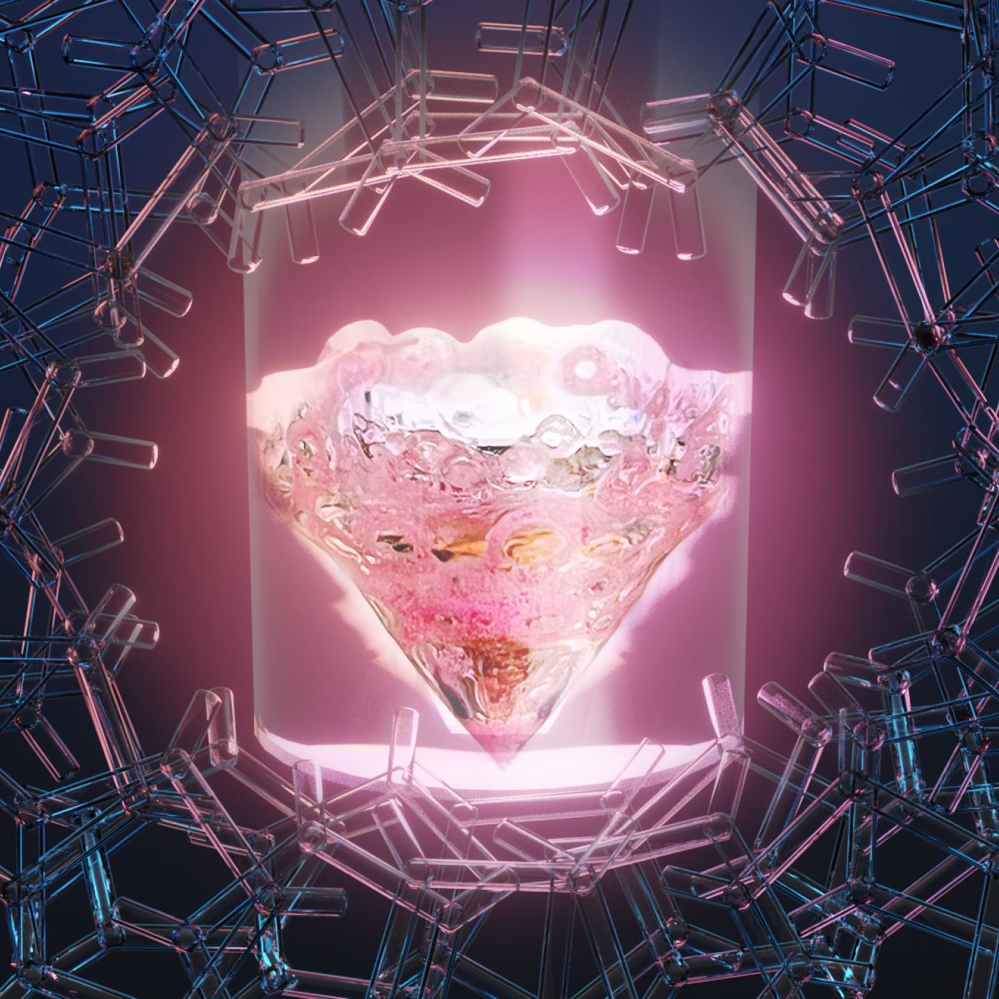
A team led by the Department of Energy’s Oak Ridge National Laboratory synthesized a tiny structure with high surface area and discovered how its unique architecture drives ions across interfaces to transport energy or information.
Scientists at Oak Ridge National Laboratory used a focused beam of electrons to stitch platinum-silicon molecules into graphene, marking the first deliberate insertion of artificial molecules into a graphene host matrix.

Rigoberto “Gobet” Advincula has been named Governor’s Chair of Advanced and Nanostructured Materials at Oak Ridge National Laboratory and the University of Tennessee.

Liam Collins was drawn to study physics to understand “hidden things” and honed his expertise in microscopy so that he could bring them to light.

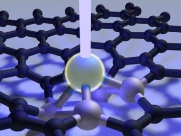
An Oak Ridge National Laboratory-led team used a scanning transmission electron microscope to selectively position single atoms below a crystal’s surface for the first time.

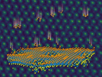
Scientists at the Department of Energy’s Oak Ridge National Laboratory induced a two-dimensional material to cannibalize itself for atomic “building blocks” from which stable structures formed. The findings, reported in Nature Communications, provide insights that ...

Sergei Kalinin of the Department of Energy’s Oak Ridge National Laboratory knows that seeing something is not the same as understanding it. As director of ORNL’s Institute for Functional Imaging of Materials, he convenes experts in microscopy and computing to gain scientific insigh...

The materials inside a fusion reactor must withstand one of the most extreme environments in science, with temperatures in the thousands of degrees Celsius and a constant bombardment of neutron radiation and deuterium and tritium, isotopes of hydrogen, from the volatile plasma at th...