
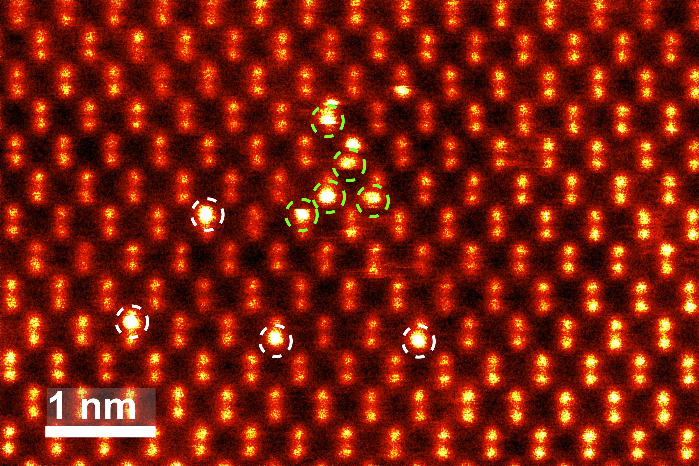
An ORNL-led team used scanning transmission electron microscopy to observed atomic transformations on the edges of pores in a two-dimensional transition metal dichalcogenide. The controlled production of nanopores with stable atomic edge structures may enable new functional applications. Credit: Xiahan Sang/Oak Ridge National Laboratory, U.S. Dept. of Energy
September 4, 2018 - An Oak Ridge National Laboratory-led team used a scanning transmission electron microscope to selectively position single atoms below a crystal’s surface for the first time. “We’re moving individual dopants where we want them to go,” said Bethany Hudak of ORNL. “Direct atom positioning represents one step toward realizing the single-atom devices potentially needed to build future quantum computers.” The researchers grew a crystal consisting of silicon atoms but containing a few bismuth atoms. The bismuth atoms’ larger size caused strain on the lattice framework of the crystal. Then, they developed a method to employ the microscope’s electron beam to selectively hit a column of silicon atoms with enough energy to eject one from its lattice position, enabling a bismuth atom to slide into the vacant spot. Next steps for the work, which was published in ACS Nano, include controlling atom placement at different crystal depths and programming the electron microscope to create specific shapes. — Dawn Levy

