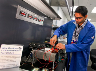
ORNL’s Power Electronics and Electric Machinery (PEEM) Laboratory is the primary laboratory for the DOE Vehicle Technologies Office electric drive research and development due to a unique combination of facilities and expertise. Focus areas include wireless and wired power charging, power inverters and converters, efficient motor control technologies, compact electric motors, and packaging. The laboratory's activities cover all these areas from invention to analysis, modeling, simulation, to building prototypes starting from a bare die, and evaluating both novel and commercial components.
The Power Electronics and Electric Machinery Laboratory has unique capabilities in power semiconductor device testing and characterization, power module and inverter packaging, converter and inverter topology development, power converter modeling, control and simulation, and rapid prototype fabrication and evaluation. PEEM has dramatically advanced the technology of advanced soft-switched inverters, multilevel inverters, current-source inverters, dc-to-dc converters, battery chargers, motor control techniques, and efficient, compact electric machines. Additionally, the laboratory is involved with high-temperature device development, innovative packaging technologies for high temperatures, and electromagnetic interference minimization, as well as the advancement and characterization of a wide variety of power semiconductor devices including silicon, silicon carbide, and gallium nitride devices.
Researchers at the NTRC leverage world-leading capabilities across ORNL including high-performance computing and materials characterization to examine materials at the atomic level, to create predictive models that accelerate the design of new components, and to predict reliability under field conditions and improve lifetime and reliability of new technologies. Capabilities include semiconductor-based device fabrication facilities that support a wide variety of thin-film and solid-state electronics R&D. Experts in the laboratory work closely with researchers at the adjacent Manufacturing Demonstration Facility, which provides access to unique additive and roll-to-roll manufacturing capabilities to accelerate the product-to-market cycle.
The PEEM Laboratory provides approximately 835 m2 (9,000 ft2) of space, including areas specifically designed for proprietary research.
R&D Focus Areas
- Advanced manufacturing of power electronics packages and heat exchangers
- Wireless charging of plug-in electric vehicles
- Power device packaging
- Wide bandgap (WBG) power device characterization and evaluation
- WBG applications
- Inverters, converters, chargers, and their thermal management
- Analysis, modeling, and simulation of power electronics and electric machines
- Prototype design and evaluation
- Novel motor designs and digital controls
- Non-rare earth motors
Equipment Highlights
- 600-volt, 600-ampere bi-directional dc power supply
- 100-hp, 10,000-rpm 4-quadrant dynamometer
- 450-hp, 15,000-rpm water brake dynamometer
- Ultra high-speed rotational equipment safety tank
- Programmable environmental oven to 750°C
- Environmental chamber with humidity control capability from −50 to 180°C
- Environmental laboratory hood
- WBG material and medium-voltage (up to approximately 1200 V) device evaluation facility including
- device and component characterization at temperatures up to 600°C
- static and dynamic measurements of diodes and switches up to 1,200 V and 400 A
- testing of devices up to 30 V gate drive and down to 10 ns switching times
- extraction of device capacitances up to 1000 V
- dynamic reverse biasing test
- leakage current measurement
- avalanche testing
- WBG high-voltage (up to 20 kV) device evaluation including
- maximum voltage and current without transformer: 2.2 kV, 0–11A
- rise time of 20 ns (to 2.2 kV), 15 ns (to 500 V); fall time: 35 ns
- pulsewidth 0.05 s to 1000 s
- pulse repetition rate single shot to 1 MHz
WBG device evaluation has been performed by ORNL in the WBG Data Analysis and Technology Assessment (DATA) facility for more than 10 years. ORNL works collaboratively with device manufacturers from around the world to assist in moving WBG device technology forward. The ORNL evaluation yields device characteristics that are then used to develop behavioral models of the devices that are, in turn, used in application models to determine system-level performance in real-world applications.
WBG device and component capabilities enable benchmarking evaluation and characterization at the bare die and packaging level as well as device modeling. High-level system modeling of power converters for motor drives is conducted to elucidate the impact of using WBG devices. ORNL collaborated with partners to build industry’s first silicon insulated-gate bipolar transistor–silicon carbonide Schottky diode hybrid 55 kW inverter, which demonstrated up to 30% efficiency improvement compared to an all-silicon module. PEEM staff have developed all–silicon carbide air-cooled inverter designs with innovative high-temperature module and heat sink designs. In the power device packaging laboratory, researchers have prototyped a variety of wide bandgap–based inverters, dc-to-dc converters, and power modules—many incorporating new geometries enabled by 3D printing.

