
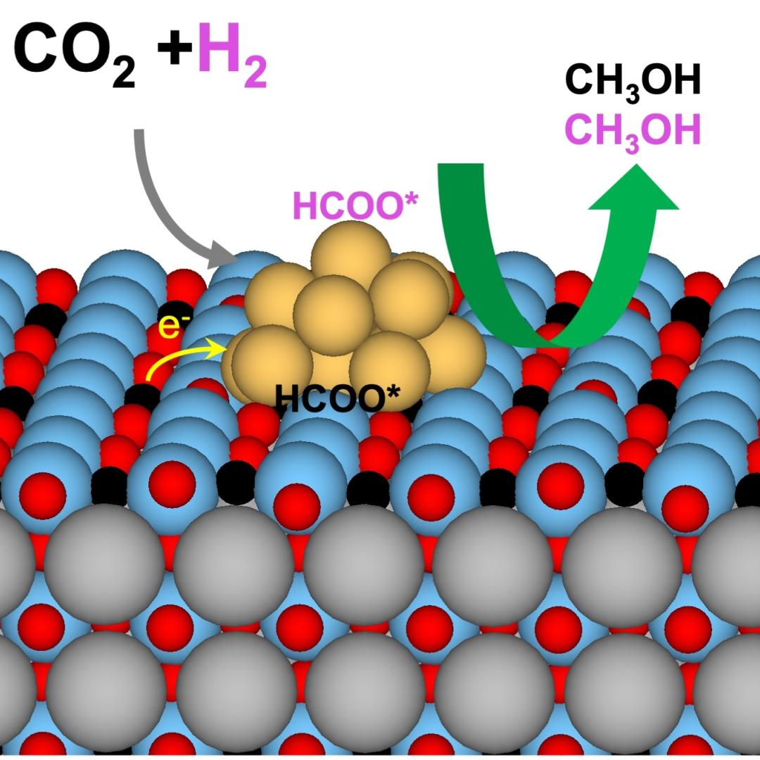

Scientists at Oak Ridge National Laboratory used a focused beam of electrons to stitch platinum-silicon molecules into graphene, marking the first deliberate insertion of artificial molecules into a graphene host matrix.

A novel approach developed by scientists at ORNL can scan massive datasets of large-scale satellite images to more accurately map infrastructure – such as buildings and roads – in hours versus days.

Rigoberto “Gobet” Advincula has been named Governor’s Chair of Advanced and Nanostructured Materials at Oak Ridge National Laboratory and the University of Tennessee.

Liam Collins was drawn to study physics to understand “hidden things” and honed his expertise in microscopy so that he could bring them to light.
Scientists at have experimentally demonstrated a novel cryogenic, or low temperature, memory cell circuit design based on coupled arrays of Josephson junctions, a technology that may be faster and more energy efficient than existing memory devices.