


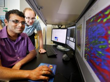
At the Department of Energy’s Oak Ridge National Laboratory, scientists use artificial intelligence, or AI, to accelerate the discovery and development of materials for energy and information technologies.
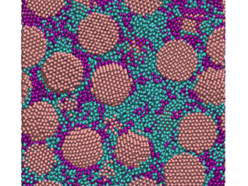
Oak Ridge National Laboratory scientists have discovered a cost-effective way to significantly improve the mechanical performance of common polymer nanocomposite materials.
Systems biologist Paul Abraham uses his fascination with proteins, the molecular machines of nature, to explore new ways to engineer more productive ecosystems and hardier bioenergy crops.

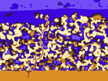
Oak Ridge National Laboratory researchers have built a novel microscope that provides a “chemical lens” for viewing biological systems including cell membranes and biofilms.

Scientists at the Department of Energy Manufacturing Demonstration Facility at ORNL have their eyes on the prize: the Transformational Challenge Reactor, or TCR, a microreactor built using 3D printing and other new approaches that will be up and running by 2023.
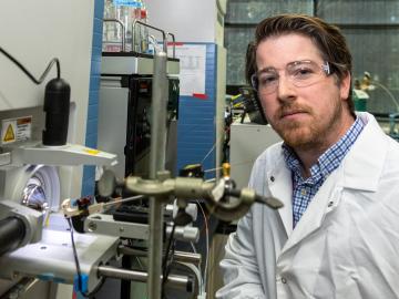
Oak Ridge National Laboratory researchers have developed a thin film, highly conductive solid-state electrolyte made of a polymer and ceramic-based composite for lithium metal batteries.

Scientists at Oak Ridge National Laboratory used a focused beam of electrons to stitch platinum-silicon molecules into graphene, marking the first deliberate insertion of artificial molecules into a graphene host matrix.

Liam Collins was drawn to study physics to understand “hidden things” and honed his expertise in microscopy so that he could bring them to light.

Scientists at have experimentally demonstrated a novel cryogenic, or low temperature, memory cell circuit design based on coupled arrays of Josephson junctions, a technology that may be faster and more energy efficient than existing memory devices.