


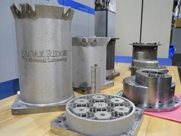
Researchers at the Department of Energy’s Oak Ridge National Laboratory are refining their design of a 3D-printed nuclear reactor core, scaling up the additive manufacturing process necessary to build it, and developing methods
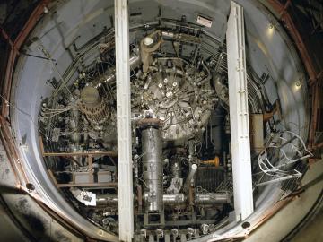
In the 1960s, Oak Ridge National Laboratory's four-year Molten Salt Reactor Experiment tested the viability of liquid fuel reactors for commercial power generation. Results from that historic experiment recently became the basis for the first-ever molten salt reactor benchmark.
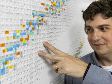
In the Physics Division of the Department of Energy’s Oak Ridge National Laboratory, James (“Mitch”) Allmond conducts experiments and uses theoretical models to advance our understanding of the structure of atomic nuclei, which are made of various combinations of protons and neutrons (nucleons).

In the race to identify solutions to the COVID-19 pandemic, researchers at the Department of Energy’s Oak Ridge National Laboratory are joining the fight by applying expertise in computational science, advanced manufacturing, data science and neutron science.

As a teenager, Kat Royston had a lot of questions. Then an advanced-placement class in physics convinced her all the answers were out there.
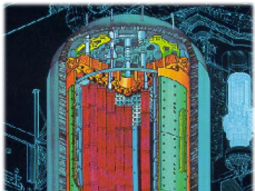
A software package, 10 years in the making, that can predict the behavior of nuclear reactors’ cores with stunning accuracy has been licensed commercially for the first time.

Rigoberto “Gobet” Advincula has been named Governor’s Chair of Advanced and Nanostructured Materials at Oak Ridge National Laboratory and the University of Tennessee.

Liam Collins was drawn to study physics to understand “hidden things” and honed his expertise in microscopy so that he could bring them to light.
Scientists at have experimentally demonstrated a novel cryogenic, or low temperature, memory cell circuit design based on coupled arrays of Josephson junctions, a technology that may be faster and more energy efficient than existing memory devices.