


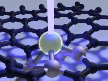
Scientists at Oak Ridge National Laboratory used a focused beam of electrons to stitch platinum-silicon molecules into graphene, marking the first deliberate insertion of artificial molecules into a graphene host matrix.

A novel approach developed by scientists at ORNL can scan massive datasets of large-scale satellite images to more accurately map infrastructure – such as buildings and roads – in hours versus days.

Rigoberto “Gobet” Advincula has been named Governor’s Chair of Advanced and Nanostructured Materials at Oak Ridge National Laboratory and the University of Tennessee.

Liam Collins was drawn to study physics to understand “hidden things” and honed his expertise in microscopy so that he could bring them to light.
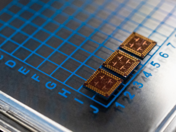
Scientists at have experimentally demonstrated a novel cryogenic, or low temperature, memory cell circuit design based on coupled arrays of Josephson junctions, a technology that may be faster and more energy efficient than existing memory devices.
Students often participate in internships and receive formal training in their chosen career fields during college, but some pursue professional development opportunities even earlier.
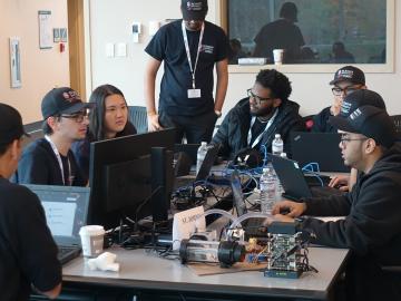
Oak Ridge National Laboratory will give college students the chance to practice cybersecurity skills in a real-world setting as a host of the Department of Energy’s fifth collegiate CyberForce Competition on Nov. 16. The event brings together student teams from across the country to compete at 10 of DOE’s national laboratories.
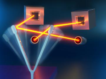
Researchers at ORNL and the National Renewable Energy Laboratory took inspiration from flying insects to demonstrate a miniaturized gyroscope, a special sensor used in navigation technologies.
Researchers at the Department of Energy’s Oak Ridge National Laboratory have received five 2019 R&D 100 Awards, increasing the lab’s total to 221 since the award’s inception in 1963.

Six new nuclear reactor technologies are set to deploy for commercial use between 2030 and 2040. Called Generation IV nuclear reactors, they will operate with improved performance at dramatically higher temperatures than today’s reactors.