Filter News
Area of Research
News Topics
- (-) Fusion (3)
- (-) Microscopy (4)
- 3-D Printing/Advanced Manufacturing (6)
- Advanced Reactors (1)
- Artificial Intelligence (1)
- Big Data (1)
- Bioenergy (2)
- Biology (1)
- Biomedical (3)
- Clean Water (1)
- Composites (2)
- Computer Science (11)
- Critical Materials (2)
- Cybersecurity (2)
- Energy Storage (1)
- Environment (3)
- Grid (1)
- Isotopes (3)
- Materials Science (9)
- Mercury (1)
- Molten Salt (3)
- Nanotechnology (8)
- Neutron Science (8)
- Nuclear Energy (9)
- Physics (8)
- Polymers (3)
- Quantum Science (3)
- Security (6)
- Space Exploration (2)
- Summit (2)
- Transportation (4)
Media Contacts
If you ask the staff and researchers at the Department of Energy’s Oak Ridge National Laboratory how they were first referred to the lab, you will get an extremely varied list of responses. Some may have come here as student interns, some grew up in the area and knew the lab by ...
An Oak Ridge National Laboratory-led team used a scanning transmission electron microscope to selectively position single atoms below a crystal’s surface for the first time.
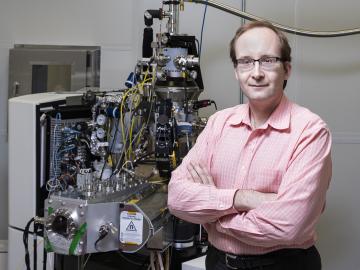
Sergei Kalinin of the Department of Energy’s Oak Ridge National Laboratory knows that seeing something is not the same as understanding it. As director of ORNL’s Institute for Functional Imaging of Materials, he convenes experts in microscopy and computing to gain scientific insigh...

The materials inside a fusion reactor must withstand one of the most extreme environments in science, with temperatures in the thousands of degrees Celsius and a constant bombardment of neutron radiation and deuterium and tritium, isotopes of hydrogen, from the volatile plasma at th...
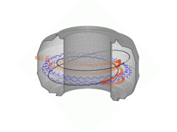
Fusion scientists from Oak Ridge National Laboratory are studying the behavior of high-energy electrons when the plasma that generates nuclear fusion energy suddenly cools during a magnetic disruption. Fusion energy is created when hydrogen isotopes are heated to millions of degrees...
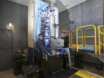
A scientific team led by the Department of Energy’s Oak Ridge National Laboratory has found a new way to take the local temperature of a material from an area about a billionth of a meter wide, or approximately 100,000 times thinner than a human hair. This discove...

Material surfaces and interfaces may appear flat and void of texture to the naked eye, but a view from the nanoscale reveals an intricate tapestry of atomic patterns that control the reactions between the material and its environment. Electron microscopy allows researchers to probe...


