


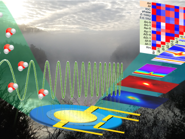
Researchers at ORNL used quantum optics to advance state-of-the-art microscopy and illuminate a path to detecting material properties with greater sensitivity than is possible with traditional tools.
An all-in-one experimental platform developed at Oak Ridge National Laboratory’s Center for Nanophase Materials Sciences accelerates research on promising materials for future technologies.

Five researchers at the Department of Energy’s Oak Ridge National Laboratory have been named ORNL Corporate Fellows in recognition of significant career accomplishments and continued leadership in their scientific fields.
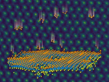
An ORNL team used a simple process to implant atoms precisely into the top layers of ultra-thin crystals, yielding two-sided structures with different chemical compositions.

In the search to create materials that can withstand extreme radiation, Yanwen Zhang, a researcher at the Department of Energy’s Oak Ridge National Laboratory, says that materials scientists must think outside the box.
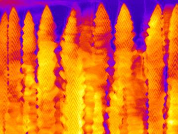
A team led by the Department of Energy’s Oak Ridge National Laboratory synthesized a tiny structure with high surface area and discovered how its unique architecture drives ions across interfaces to transport energy or information.

In the Physics Division of the Department of Energy’s Oak Ridge National Laboratory, James (“Mitch”) Allmond conducts experiments and uses theoretical models to advance our understanding of the structure of atomic nuclei, which are made of various combinations of protons and neutrons (nucleons).

Rigoberto “Gobet” Advincula has been named Governor’s Chair of Advanced and Nanostructured Materials at Oak Ridge National Laboratory and the University of Tennessee.

Liam Collins was drawn to study physics to understand “hidden things” and honed his expertise in microscopy so that he could bring them to light.