


Scientists at Oak Ridge National Laboratory used new techniques to create a composite that increases the electrical current capacity of copper wires, providing a new material that can be scaled for use in ultra-efficient, power-dense electric vehicle traction motors.
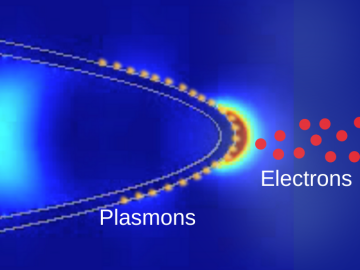
Scientists at ORNL and the University of Nebraska have developed an easier way to generate electrons for nanoscale imaging and sensing, providing a useful new tool for material science, bioimaging and fundamental quantum research.
Systems biologist Paul Abraham uses his fascination with proteins, the molecular machines of nature, to explore new ways to engineer more productive ecosystems and hardier bioenergy crops.
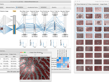
From materials science and earth system modeling to quantum information science and cybersecurity, experts in many fields run simulations and conduct experiments to collect the abundance of data necessary for scientific progress.
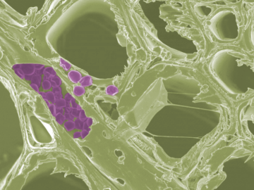
Scientists at the Department of Energy’s Oak Ridge National Laboratory have developed a new method to peer deep into the nanostructure of biomaterials without damaging the sample. This novel technique can confirm structural features in starch, a carbohydrate important in biofuel production.

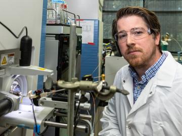
Liam Collins was drawn to study physics to understand “hidden things” and honed his expertise in microscopy so that he could bring them to light.

Scientists at have experimentally demonstrated a novel cryogenic, or low temperature, memory cell circuit design based on coupled arrays of Josephson junctions, a technology that may be faster and more energy efficient than existing memory devices.