


Liam Collins was drawn to study physics to understand “hidden things” and honed his expertise in microscopy so that he could bring them to light.

A typhoon strikes an island in the Pacific Ocean, downing power lines and cell towers. An earthquake hits a remote mountainous region, destroying structures and leaving no communication infrastructure behind.
Scientists at have experimentally demonstrated a novel cryogenic, or low temperature, memory cell circuit design based on coupled arrays of Josephson junctions, a technology that may be faster and more energy efficient than existing memory devices.
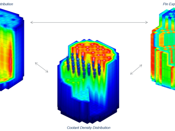
Nuclear scientists at Oak Ridge National Laboratory have established a Nuclear Quality Assurance-1 program for a software product designed to simulate today’s commercial nuclear reactors – removing a significant barrier for industry adoption of the technology.

To better determine the potential energy cost savings among connected homes, researchers at Oak Ridge National Laboratory developed a computer simulation to more accurately compare energy use on similar weather days.