

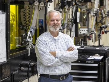
Porter Bailey started and will end his 33-year career at ORNL in the same building: 7920 of the Radiochemical Engineering Development Center.
Scientists at Oak Ridge National Laboratory and the University of Tennessee designed and demonstrated a method to make carbon-based materials that can be used as electrodes compatible with a specific semiconductor circuitry.
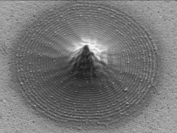
An all-in-one experimental platform developed at Oak Ridge National Laboratory’s Center for Nanophase Materials Sciences accelerates research on promising materials for future technologies.

Oak Ridge National Laboratory researchers have discovered a better way to separate actinium-227, a rare isotope essential for an FDA-approved cancer treatment.
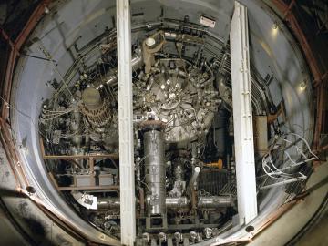
In the 1960s, Oak Ridge National Laboratory's four-year Molten Salt Reactor Experiment tested the viability of liquid fuel reactors for commercial power generation. Results from that historic experiment recently became the basis for the first-ever molten salt reactor benchmark.
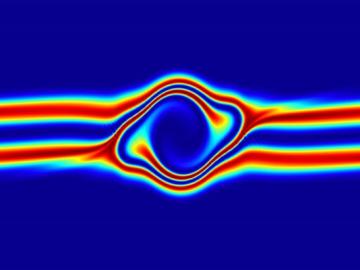
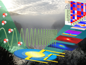
The prospect of simulating a fusion plasma is a step closer to reality thanks to a new computational tool developed by scientists in fusion physics, computer science and mathematics at ORNL.

Liam Collins was drawn to study physics to understand “hidden things” and honed his expertise in microscopy so that he could bring them to light.