Light moves through a fiber and stimulates the metal electrons in nanotip into collective oscillations called surface plasmons, assisting electrons to leave the tip. This simple electron nano-gun can be made more versatile via different forms of material composition and structuring. Credit: Ali Passian/ORNL, U.S. Dept. of Energy

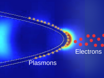
Scientists at ORNL and the University of Nebraska have developed an easier way to generate electrons for nanoscale imaging and sensing, providing a useful new tool for material science, bioimaging and fundamental quantum research.

Starch granules

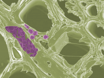
Scientists at the Department of Energy’s Oak Ridge National Laboratory have developed a new method to peer deep into the nanostructure of biomaterials without damaging the sample. This novel technique can confirm structural features in starch, a carbohydrate important in biofuel production.

Scanning probe microscopes use an atom-sharp tip—only a few nanometers thick—to image materials on a nanometer length scale. The probe tip, invisible to the eye, is attached to a cantilever (pictured) that moves across material surfaces like the tone arm on a record player. Credit: Genevieve Martin/Oak Ridge National Laboratory; U.S. Dept. of Energy.

Liam Collins was drawn to study physics to understand “hidden things” and honed his expertise in microscopy so that he could bring them to light.

ORNL-developed cryogenic memory cell circuit designs fabricated onto these small chips by SeeQC, a superconducting technology company, successfully demonstrated read, write and reset memory functions. Credit: Carlos Jones/Oak Ridge National Laboratory, U.S. Dept. of Energy

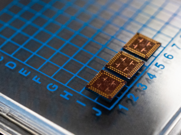
Scientists at have experimentally demonstrated a novel cryogenic, or low temperature, memory cell circuit design based on coupled arrays of Josephson junctions, a technology that may be faster and more energy efficient than existing memory devices.