![White car (Porsche Taycan) with the hood popped is inside the building with an american flag on the wall.](/sites/default/files/styles/featured_square_large/public/2024-06/2024-P09317.jpg?h=8f9cfe54&itok=m6sQhZRq)
Filter News
Area of Research
- (-) Materials (34)
- Advanced Manufacturing (5)
- Biology and Environment (14)
- Clean Energy (40)
- Climate and Environmental Systems (2)
- Computer Science (2)
- Fusion and Fission (5)
- Fusion Energy (5)
- Isotopes (1)
- Materials for Computing (3)
- National Security (4)
- Neutron Science (16)
- Nuclear Science and Technology (18)
- Nuclear Systems Modeling, Simulation and Validation (1)
- Quantum information Science (1)
- Supercomputing (21)
News Topics
- (-) 3-D Printing/Advanced Manufacturing (4)
- (-) Advanced Reactors (1)
- (-) Biomedical (1)
- (-) Climate Change (1)
- (-) Materials Science (31)
- (-) Molten Salt (1)
- (-) Nanotechnology (12)
- Artificial Intelligence (2)
- Big Data (2)
- Bioenergy (3)
- Chemical Sciences (2)
- Computer Science (8)
- Coronavirus (1)
- Critical Materials (2)
- Cybersecurity (1)
- Energy Storage (9)
- Environment (3)
- Exascale Computing (1)
- Isotopes (1)
- Machine Learning (3)
- Materials (1)
- Mathematics (1)
- Microscopy (6)
- National Security (1)
- Neutron Science (10)
- Nuclear Energy (3)
- Physics (8)
- Polymers (4)
- Quantum Science (4)
- Security (1)
- Summit (2)
- Sustainable Energy (5)
- Transformational Challenge Reactor (2)
- Transportation (3)
Media Contacts
![Gobet_Advincula Portrait](/sites/default/files/styles/list_page_thumbnail/public/2020-02/2020-P00191.png?h=8f9cfe54&itok=MA0hIqj6)
Rigoberto “Gobet” Advincula has been named Governor’s Chair of Advanced and Nanostructured Materials at Oak Ridge National Laboratory and the University of Tennessee.
![Scanning probe microscopes use an atom-sharp tip—only a few nanometers thick—to image materials on a nanometer length scale. The probe tip, invisible to the eye, is attached to a cantilever (pictured) that moves across material surfaces like the tone arm on a record player. Credit: Genevieve Martin/Oak Ridge National Laboratory; U.S. Dept. of Energy.](/sites/default/files/styles/list_page_thumbnail/public/2020-01/2019-P15115.jpg?h=c6980913&itok=o69jyoNw)
Liam Collins was drawn to study physics to understand “hidden things” and honed his expertise in microscopy so that he could bring them to light.
![ORNL-developed cryogenic memory cell circuit designs fabricated onto these small chips by SeeQC, a superconducting technology company, successfully demonstrated read, write and reset memory functions. Credit: Carlos Jones/Oak Ridge National Laboratory, U.S. Dept. of Energy](/sites/default/files/styles/list_page_thumbnail/public/2020-01/2019-P17636.png?h=39b94f55&itok=udTwXJwT)
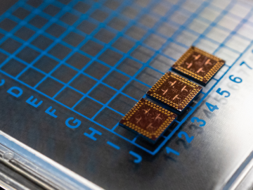
Scientists at have experimentally demonstrated a novel cryogenic, or low temperature, memory cell circuit design based on coupled arrays of Josephson junctions, a technology that may be faster and more energy efficient than existing memory devices.
![ORNL’s Xiahan Sang unambiguously resolved the atomic structure of MXene, a 2D material promising for energy storage, catalysis and electronic conductivity. Image credit: Oak Ridge National Laboratory, U.S. Dept. of Energy; photographer Carlos Jones ORNL’s Xiahan Sang unambiguously resolved the atomic structure of MXene, a 2D material promising for energy storage, catalysis and electronic conductivity. Image credit: Oak Ridge National Laboratory, U.S. Dept. of Energy; photographer Carlos Jones](/sites/default/files/styles/list_page_thumbnail/public/Sang_2016-P07680_0.jpg?itok=w0e5eR_U)
Researchers have long sought electrically conductive materials for economical energy-storage devices. Two-dimensional (2D) ceramics called MXenes are contenders. Unlike most 2D ceramics, MXenes have inherently good conductivity because they are molecular sheets made from the carbides ...