Gobet_Advincula Portrait

Rigoberto “Gobet” Advincula has been named Governor’s Chair of Advanced and Nanostructured Materials at Oak Ridge National Laboratory and the University of Tennessee.

Scanning probe microscopes use an atom-sharp tip—only a few nanometers thick—to image materials on a nanometer length scale. The probe tip, invisible to the eye, is attached to a cantilever (pictured) that moves across material surfaces like the tone arm on a record player. Credit: Genevieve Martin/Oak Ridge National Laboratory; U.S. Dept. of Energy.

Liam Collins was drawn to study physics to understand “hidden things” and honed his expertise in microscopy so that he could bring them to light.

ORNL-developed cryogenic memory cell circuit designs fabricated onto these small chips by SeeQC, a superconducting technology company, successfully demonstrated read, write and reset memory functions. Credit: Carlos Jones/Oak Ridge National Laboratory, U.S. Dept. of Energy

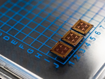
Scientists at have experimentally demonstrated a novel cryogenic, or low temperature, memory cell circuit design based on coupled arrays of Josephson junctions, a technology that may be faster and more energy efficient than existing memory devices.