Filter News
Area of Research
News Type
News Topics
- (-) Bioenergy (1)
- (-) Biomedical (1)
- (-) Environment (3)
- (-) Exascale Computing (1)
- (-) Fusion (6)
- (-) Nanotechnology (6)
- (-) Neutron Science (8)
- (-) Transportation (2)
- 3-D Printing/Advanced Manufacturing (5)
- Advanced Reactors (4)
- Artificial Intelligence (2)
- Big Data (2)
- Chemical Sciences (2)
- Climate Change (1)
- Computer Science (7)
- Coronavirus (2)
- Cybersecurity (2)
- Energy Storage (3)
- Isotopes (2)
- Machine Learning (3)
- Materials (1)
- Materials Science (13)
- Mathematics (1)
- Microscopy (1)
- Molten Salt (1)
- National Security (1)
- Nuclear Energy (14)
- Physics (7)
- Security (1)
- Space Exploration (1)
- Summit (1)
- Sustainable Energy (1)
- Transformational Challenge Reactor (3)
Media Contacts

Liam Collins was drawn to study physics to understand “hidden things” and honed his expertise in microscopy so that he could bring them to light.

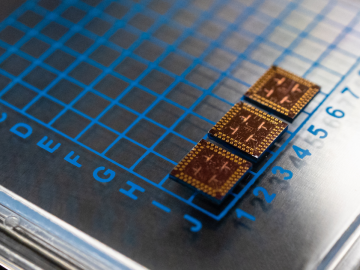
Scientists at have experimentally demonstrated a novel cryogenic, or low temperature, memory cell circuit design based on coupled arrays of Josephson junctions, a technology that may be faster and more energy efficient than existing memory devices.


