


At the Department of Energy’s Oak Ridge National Laboratory, scientists use artificial intelligence, or AI, to accelerate the discovery and development of materials for energy and information technologies.

Researchers at ORNL used quantum optics to advance state-of-the-art microscopy and illuminate a path to detecting material properties with greater sensitivity than is possible with traditional tools.

Five researchers at the Department of Energy’s Oak Ridge National Laboratory have been named ORNL Corporate Fellows in recognition of significant career accomplishments and continued leadership in their scientific fields.

Liam Collins was drawn to study physics to understand “hidden things” and honed his expertise in microscopy so that he could bring them to light.

OAK RIDGE, Tenn., March 22, 2019 – Karren Leslie More, a researcher at the Department of Energy’s Oak Ridge National Laboratory, has been elected fellow of the Microscopy Society of America (MSA) professional organization.

OAK RIDGE, Tenn., Jan. 31, 2019—A new electron microscopy technique that detects the subtle changes in the weight of proteins at the nanoscale—while keeping the sample intact—could open a new pathway for deeper, more comprehensive studies of the basic building blocks of life.

A new microscopy technique developed at the University of Illinois at Chicago allows researchers to visualize liquids at the nanoscale level — about 10 times more resolution than with traditional transmission electron microscopy — for the first time. By trapping minute amounts of...

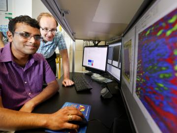
A scientific team led by the Department of Energy’s Oak Ridge National Laboratory has found a new way to take the local temperature of a material from an area about a billionth of a meter wide, or approximately 100,000 times thinner than a human hair. This discove...

Researchers have long sought electrically conductive materials for economical energy-storage devices. Two-dimensional (2D) ceramics called MXenes are contenders. Unlike most 2D ceramics, MXenes have inherently good conductivity because they are molecular sheets made from the carbides ...