Filter News
Area of Research
- (-) Materials (14)
- Biological Systems (1)
- Biology and Environment (47)
- Biology and Soft Matter (1)
- Clean Energy (24)
- Climate and Environmental Systems (1)
- Fusion and Fission (4)
- Materials for Computing (5)
- National Security (11)
- Neutron Science (5)
- Nuclear Science and Technology (5)
- Quantum information Science (2)
- Supercomputing (19)
News Topics
- (-) Advanced Reactors (1)
- (-) Bioenergy (2)
- (-) Microscopy (6)
- (-) Nanotechnology (8)
- (-) Security (1)
- 3-D Printing/Advanced Manufacturing (4)
- Artificial Intelligence (4)
- Big Data (2)
- Biomedical (2)
- Buildings (1)
- Chemical Sciences (7)
- Clean Water (2)
- Composites (2)
- Computer Science (8)
- Coronavirus (1)
- Cybersecurity (1)
- Decarbonization (1)
- Energy Storage (6)
- Environment (6)
- Exascale Computing (1)
- Fusion (2)
- Grid (2)
- High-Performance Computing (1)
- Isotopes (6)
- Machine Learning (2)
- Materials (19)
- Materials Science (17)
- Mathematics (1)
- Neutron Science (9)
- Nuclear Energy (9)
- Partnerships (3)
- Physics (11)
- Polymers (4)
- Quantum Computing (1)
- Space Exploration (1)
- Summit (1)
- Sustainable Energy (2)
- Transformational Challenge Reactor (2)
- Transportation (4)
Media Contacts

Liam Collins was drawn to study physics to understand “hidden things” and honed his expertise in microscopy so that he could bring them to light.

Students often participate in internships and receive formal training in their chosen career fields during college, but some pursue professional development opportunities even earlier.

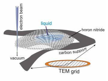
A new microscopy technique developed at the University of Illinois at Chicago allows researchers to visualize liquids at the nanoscale level — about 10 times more resolution than with traditional transmission electron microscopy — for the first time. By trapping minute amounts of...

Researchers have long sought electrically conductive materials for economical energy-storage devices. Two-dimensional (2D) ceramics called MXenes are contenders. Unlike most 2D ceramics, MXenes have inherently good conductivity because they are molecular sheets made from the carbides ...


