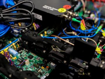
For the second year in a row, a team from the Department of Energy’s Oak Ridge and Los Alamos national laboratories led a demonstration hosted by EPB, a community-based utility and telecommunications company serving Chattanooga, Tennessee.
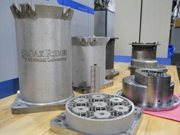
Researchers at the Department of Energy’s Oak Ridge National Laboratory are refining their design of a 3D-printed nuclear reactor core, scaling up the additive manufacturing process necessary to build it, and developing methods

Rigoberto “Gobet” Advincula has been named Governor’s Chair of Advanced and Nanostructured Materials at Oak Ridge National Laboratory and the University of Tennessee.

Liam Collins was drawn to study physics to understand “hidden things” and honed his expertise in microscopy so that he could bring them to light.