

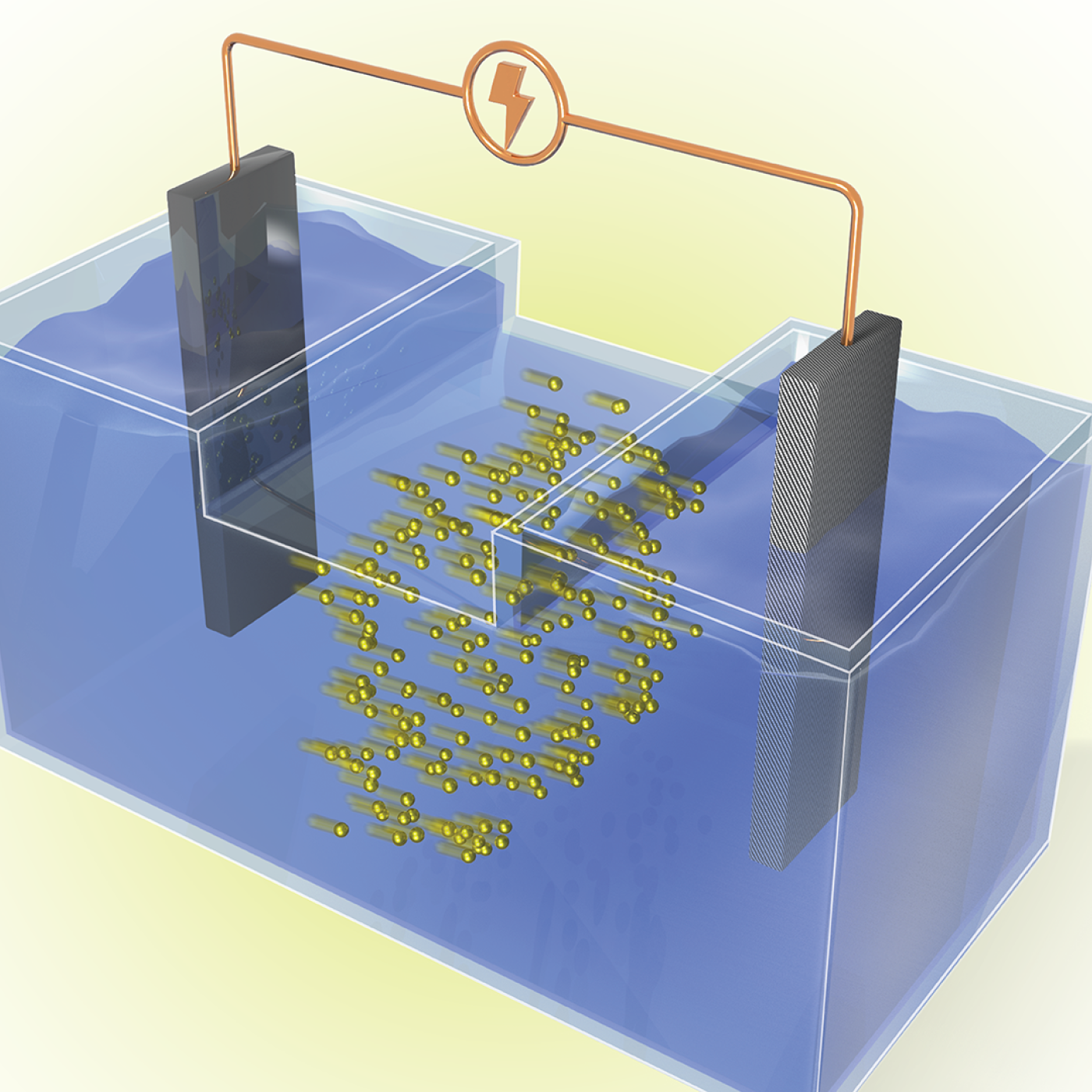
Scientists at Oak Ridge National Laboratory and the University of Tennessee designed and demonstrated a method to make carbon-based materials that can be used as electrodes compatible with a specific semiconductor circuitry.

An all-in-one experimental platform developed at Oak Ridge National Laboratory’s Center for Nanophase Materials Sciences accelerates research on promising materials for future technologies.
Oak Ridge National Laboratory researchers have built a novel microscope that provides a “chemical lens” for viewing biological systems including cell membranes and biofilms.

Scientists at Oak Ridge National Laboratory used a focused beam of electrons to stitch platinum-silicon molecules into graphene, marking the first deliberate insertion of artificial molecules into a graphene host matrix.
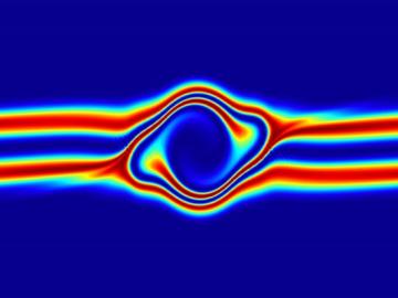
The prospect of simulating a fusion plasma is a step closer to reality thanks to a new computational tool developed by scientists in fusion physics, computer science and mathematics at ORNL.