
Filter News
Area of Research
News Topics
- (-) Computer Science (9)
- (-) Microscopy (3)
- (-) Molten Salt (1)
- (-) Nanotechnology (4)
- 3-D Printing/Advanced Manufacturing (7)
- Advanced Reactors (2)
- Big Data (2)
- Biomedical (1)
- Clean Water (2)
- Composites (1)
- Critical Materials (1)
- Energy Storage (3)
- Environment (7)
- Fusion (2)
- Grid (2)
- Isotopes (1)
- Materials Science (12)
- Mercury (1)
- Neutron Science (3)
- Nuclear Energy (5)
- Physics (2)
- Polymers (3)
- Space Exploration (3)
- Summit (2)
- Sustainable Energy (2)
- Transportation (8)
Media Contacts

A team of scientists led by Oak Ridge National Laboratory used machine learning methods to generate a high-resolution map of vegetation growing in the remote reaches of the Alaskan tundra.
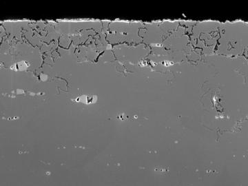
Oak Ridge National Laboratory scientists analyzed more than 50 years of data showing puzzlingly inconsistent trends about corrosion of structural alloys in molten salts and found one factor mattered most—salt purity.

Scientists at Oak Ridge National Laboratory and Hypres, a digital superconductor company, have tested a novel cryogenic, or low-temperature, memory cell circuit design that may boost memory storage while using less energy in future exascale and quantum computing applications.
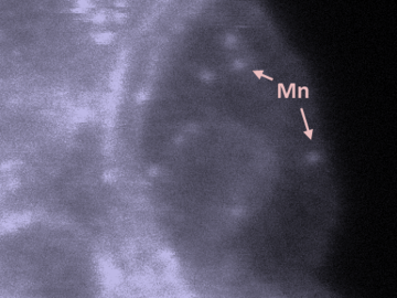
Oak Ridge National Laboratory scientists studying fuel cells as a potential alternative to internal combustion engines used sophisticated electron microscopy to investigate the benefits of replacing high-cost platinum with a lower cost, carbon-nitrogen-manganese-based catalyst.
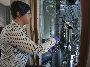
An Oak Ridge National Laboratory-led team used a scanning transmission electron microscope to selectively position single atoms below a crystal’s surface for the first time.
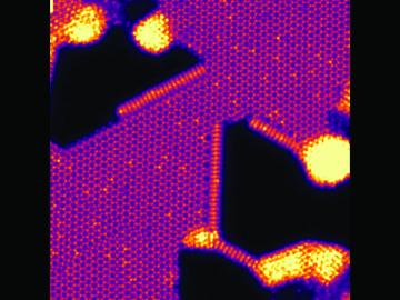
An Oak Ridge National Laboratory–led team has learned how to engineer tiny pores embellished with distinct edge structures inside atomically-thin two-dimensional, or 2D, crystals. The 2D crystals are envisioned as stackable building blocks for ultrathin electronics and other advance...


