

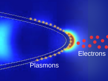
Scientists at ORNL and the University of Nebraska have developed an easier way to generate electrons for nanoscale imaging and sensing, providing a useful new tool for material science, bioimaging and fundamental quantum research.
From materials science and earth system modeling to quantum information science and cybersecurity, experts in many fields run simulations and conduct experiments to collect the abundance of data necessary for scientific progress.

Scientists at the Department of Energy Manufacturing Demonstration Facility at ORNL have their eyes on the prize: the Transformational Challenge Reactor, or TCR, a microreactor built using 3D printing and other new approaches that will be up and running by 2023.

In the race to identify solutions to the COVID-19 pandemic, researchers at the Department of Energy’s Oak Ridge National Laboratory are joining the fight by applying expertise in computational science, advanced manufacturing, data science and neutron science.
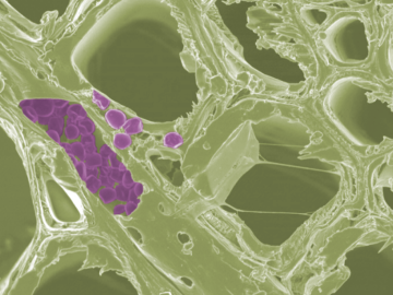
Scientists at the Department of Energy’s Oak Ridge National Laboratory have developed a new method to peer deep into the nanostructure of biomaterials without damaging the sample. This novel technique can confirm structural features in starch, a carbohydrate important in biofuel production.

Liam Collins was drawn to study physics to understand “hidden things” and honed his expertise in microscopy so that he could bring them to light.

A new microscopy technique developed at the University of Illinois at Chicago allows researchers to visualize liquids at the nanoscale level — about 10 times more resolution than with traditional transmission electron microscopy — for the first time. By trapping minute amounts of...