


Liam Collins was drawn to study physics to understand “hidden things” and honed his expertise in microscopy so that he could bring them to light.

To better determine the potential energy cost savings among connected homes, researchers at Oak Ridge National Laboratory developed a computer simulation to more accurately compare energy use on similar weather days.
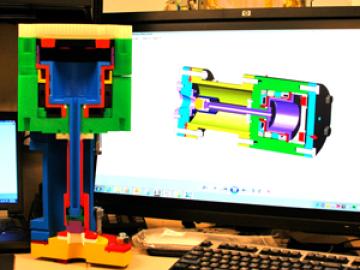
ITER, the international fusion research facility now under construction in St. Paul-lez-Durance, France, has been called a puzzle of a million pieces. US ITER staff at Oak Ridge National Laboratory are using an affordable tool—desktop three-dimensional printing, also known as additive printing—to help them design and configure components more efficiently and affordably.
Through a network that consists of hundreds of low-cost monitors that plug into standard 110-volt outlets, GridEye can play a role in ensuring the reliability of the nation's power grids. The system, developed by researchers at Oak Ridge National Laboratory, provides real-time information about dyna...