


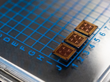
Scientists at have experimentally demonstrated a novel cryogenic, or low temperature, memory cell circuit design based on coupled arrays of Josephson junctions, a technology that may be faster and more energy efficient than existing memory devices.

Researchers across the scientific spectrum crave data, as it is essential to understanding the natural world and, by extension, accelerating scientific progress.
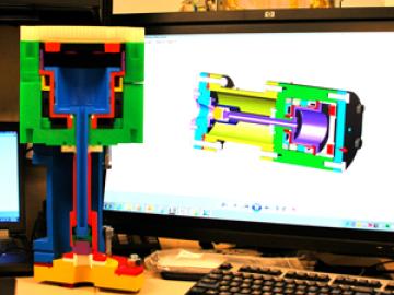
ITER, the international fusion research facility now under construction in St. Paul-lez-Durance, France, has been called a puzzle of a million pieces. US ITER staff at Oak Ridge National Laboratory are using an affordable tool—desktop three-dimensional printing, also known as additive printing—to help them design and configure components more efficiently and affordably.