31 - 40 of 42 Results

Important of the application is enabling a cost-effective precision manufacturing method Current technology is limited to injection molded individual pi-joints limiting control of pi-joint direction, this creates hurdle in introducing high volume production to the composite in
This technology aims to provide and integrated and oxidation resistant cladding or coating onto carbon-based composites in seconds.
This invention demonstrates the strong potential for hybridization of CNF with natural fibers for facile drying and inclusion of the CNF into polymer matrices for high performance composites.
This technology provides a device, platform and method of fabrication of new atomically tailored materials. This “synthescope” is a scanning transmission electron microscope (STEM) transformed into an atomic-scale material manipulation platform.


Silicon nitride fiber is a critical material mainly used in the aerospace industry but has many applications. This fiber is prized for its properties, as it is transparent to electromagnetic radiation but allows signals to go through it.
This technology combines 3D printing and compression molding to produce high-strength, low-porosity composite articles.

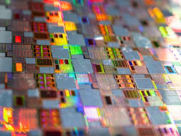
This invention presents technologies for characterizing physical properties of a sample's surface by combining image processing with machine learning techniques.

This invention introduces a system for microscopy called pan-sharpening, enabling the generation of images with both full-spatial and full-spectral resolution without needing to capture the entire dataset, significantly reducing data acquisition time.