Filter News
Area of Research
- (-) Materials (153)
- Advanced Manufacturing (11)
- Biology and Environment (57)
- Building Technologies (2)
- Clean Energy (120)
- Computational Biology (1)
- Computational Engineering (1)
- Computer Science (9)
- Electricity and Smart Grid (1)
- Energy Frontier Research Centers (1)
- Energy Sciences (1)
- Functional Materials for Energy (2)
- Fusion and Fission (9)
- Fusion Energy (3)
- Isotopes (4)
- Materials Characterization (2)
- Materials for Computing (19)
- Materials Under Extremes (1)
- National Security (33)
- Neutron Science (39)
- Nuclear Science and Technology (4)
- Quantum information Science (4)
- Supercomputing (70)
News Topics
- (-) Artificial Intelligence (9)
- (-) Composites (9)
- (-) Cybersecurity (4)
- (-) Materials (73)
- (-) Microscopy (27)
- (-) Nanotechnology (39)
- (-) Physics (29)
- (-) Sustainable Energy (13)
- 3-D Printing/Advanced Manufacturing (23)
- Advanced Reactors (4)
- Big Data (2)
- Bioenergy (11)
- Biology (4)
- Biomedical (7)
- Buildings (5)
- Chemical Sciences (32)
- Clean Water (3)
- Climate Change (5)
- Computer Science (17)
- Coronavirus (4)
- Critical Materials (13)
- Decarbonization (7)
- Energy Storage (34)
- Environment (15)
- Exascale Computing (2)
- Frontier (3)
- Fusion (7)
- Grid (5)
- High-Performance Computing (4)
- Irradiation (1)
- Isotopes (13)
- ITER (1)
- Machine Learning (5)
- Materials Science (78)
- Mathematics (1)
- Molten Salt (3)
- National Security (3)
- Net Zero (1)
- Neutron Science (33)
- Nuclear Energy (16)
- Partnerships (11)
- Polymers (17)
- Quantum Computing (3)
- Quantum Science (11)
- Renewable Energy (1)
- Security (2)
- Simulation (1)
- Space Exploration (2)
- Summit (2)
- Transformational Challenge Reactor (3)
- Transportation (14)
Media Contacts

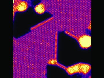
An Oak Ridge National Laboratory–led team has learned how to engineer tiny pores embellished with distinct edge structures inside atomically-thin two-dimensional, or 2D, crystals. The 2D crystals are envisioned as stackable building blocks for ultrathin electronics and other advance...

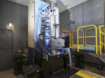
A scientific team led by the Department of Energy’s Oak Ridge National Laboratory has found a new way to take the local temperature of a material from an area about a billionth of a meter wide, or approximately 100,000 times thinner than a human hair. This discove...

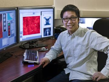
Researchers have long sought electrically conductive materials for economical energy-storage devices. Two-dimensional (2D) ceramics called MXenes are contenders. Unlike most 2D ceramics, MXenes have inherently good conductivity because they are molecular sheets made from the carbides ...


