1 - 10 of 14 Results
Dual-GP addresses limitations in traditional GPBO-driven autonomous experimentation by incorporating an additional surrogate observer and allowing human oversight, this technique improves optimization efficiency via data quality assessment and adaptability to unanticipated exp
Currently available cast Al alloys are not suitable for various high-performance conductor applications, such as rotor, inverter, windings, busbar, heat exchangers/sinks, etc.
The invented alloys are a new family of Al-Mg alloys. This new family of Al-based alloys demonstrate an excellent ductility (10 ± 2 % elongation) despite the high content of impurities commonly observed in recycled aluminum.

The invention introduces a novel, customizable method to create, manipulate, and erase polar topological structures in ferroelectric materials using atomic force microscopy.

Scanning transmission electron microscopes are useful for a variety of applications. Atomic defects in materials are critical for areas such as quantum photonics, magnetic storage, and catalysis.

A human-in-the-loop machine learning (hML) technology potentially enhances experimental workflows by integrating human expertise with AI automation.
When a magnetic field is applied to a type-II superconductor, it penetrates the superconductor in a thin cylindrical line known as a vortex line. Traditional methods to manipulate these vortices are limited in precision and affect a broad area.
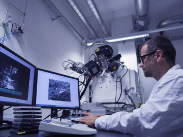
The scanning transmission electron microscope (STEM) provides unprecedented spatial resolution and is critical for many applications, primarily for imaging matter at the atomic and nanoscales and obtaining spectroscopic information at similar length scales.
Molecular Beam Epitaxy is a traditional technique for the synthesis of thin film materials used in the semiconducting and microelectronics industry. In its essence, the MBE technique heats crucibles filled with ultra-pure atomic elements under ultra high vacuum condition