1 - 10 of 11 Results

Currently available cast Al alloys are not suitable for various high-performance conductor applications, such as rotor, inverter, windings, busbar, heat exchangers/sinks, etc.
The invented alloys are a new family of Al-Mg alloys. This new family of Al-based alloys demonstrate an excellent ductility (10 ± 2 % elongation) despite the high content of impurities commonly observed in recycled aluminum.
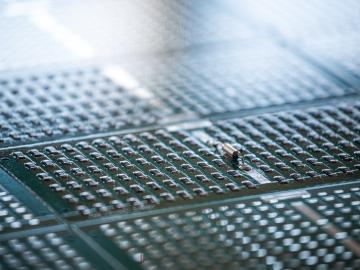
System and method for part porosity monitoring of additively manufactured components using machining
In additive manufacturing, choice of process parameters for a given material and geometry can result in porosities in the build volume, which can result in scrap.

The invention introduces a novel, customizable method to create, manipulate, and erase polar topological structures in ferroelectric materials using atomic force microscopy.
High coercive fields prevalent in wurtzite ferroelectrics present a significant challenge, as they hinder efficient polarization switching, which is essential for microelectronic applications.
Sensing of additive manufacturing processes promises to facilitate detailed quality inspection at scales that have seldom been seen in traditional manufacturing processes.

This invention presents technologies for characterizing physical properties of a sample's surface by combining image processing with machine learning techniques.

This invention introduces a system for microscopy called pan-sharpening, enabling the generation of images with both full-spatial and full-spectral resolution without needing to capture the entire dataset, significantly reducing data acquisition time.
An innovative low-cost system for in-situ monitoring of strain and temperature during directed energy deposition.
A high-strength, heat-resistant Al-Ce-Ni alloy optimized for additive manufacturing in industrial applications.