1 - 10 of 15 Results
Dual-GP addresses limitations in traditional GPBO-driven autonomous experimentation by incorporating an additional surrogate observer and allowing human oversight, this technique improves optimization efficiency via data quality assessment and adaptability to unanticipated exp
Among the methods for point source carbon capture, the absorption of CO2 using aqueous amines (namely MEA) from the post-combustion gas stream is currently considered the most promising.

The invention introduces a novel, customizable method to create, manipulate, and erase polar topological structures in ferroelectric materials using atomic force microscopy.

Scanning transmission electron microscopes are useful for a variety of applications. Atomic defects in materials are critical for areas such as quantum photonics, magnetic storage, and catalysis.
The QVis Quantum Device Circuit Optimization Module gives users the ability to map a circuit to a specific quantum devices based on the device specifications.
QVis is a visual analytics tool that helps uncover temporal and multivariate variations in noise properties of quantum devices.

A human-in-the-loop machine learning (hML) technology potentially enhances experimental workflows by integrating human expertise with AI automation.
This work seeks to alter the interface condition through thermal history modification, deposition energy density, and interface surface preparation to prevent interface cracking.
Additive manufacturing (AM) enables the incremental buildup of monolithic components with a variety of materials, and material deposition locations.
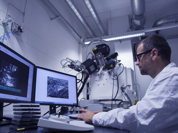
The scanning transmission electron microscope (STEM) provides unprecedented spatial resolution and is critical for many applications, primarily for imaging matter at the atomic and nanoscales and obtaining spectroscopic information at similar length scales.