1 - 10 of 28 Results
The ever-changing cellular communication landscape makes it difficult to identify, map, and localize commercial and private cellular base stations (PCBS).
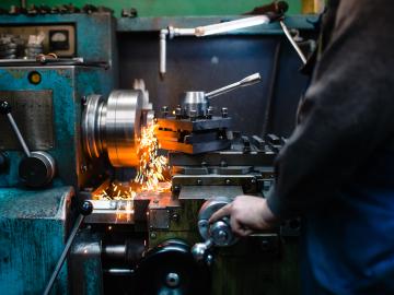
System and method for part porosity monitoring of additively manufactured components using machining
In additive manufacturing, choice of process parameters for a given material and geometry can result in porosities in the build volume, which can result in scrap.
Distortion generated during additive manufacturing of metallic components affect the build as well as the baseplate geometries. These distortions are significant enough to disqualify components for functional purposes.

The invention introduces a novel, customizable method to create, manipulate, and erase polar topological structures in ferroelectric materials using atomic force microscopy.
For additive manufacturing of large-scale parts, significant distortion can result from residual stresses during deposition and cooling. This can result in part scraps if the final part geometry is not contained in the additively manufactured preform.
High coercive fields prevalent in wurtzite ferroelectrics present a significant challenge, as they hinder efficient polarization switching, which is essential for microelectronic applications.
Distortion in scanning tunneling microscope (STM) images is an unavoidable problem. This technology is an algorithm to identify and correct distorted wavefronts in atomic resolution STM images.
The QVis Quantum Device Circuit Optimization Module gives users the ability to map a circuit to a specific quantum devices based on the device specifications.
QVis is a visual analytics tool that helps uncover temporal and multivariate variations in noise properties of quantum devices.