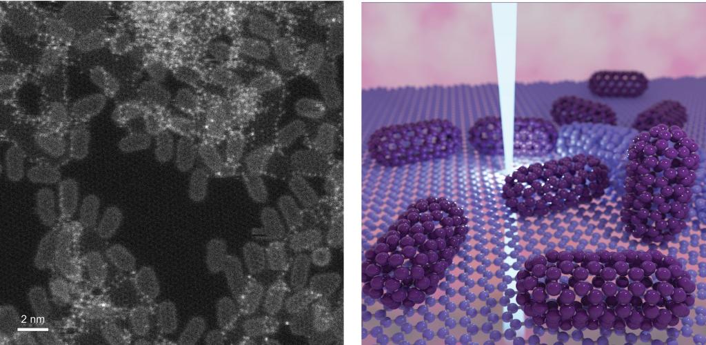
The mission of the STEM group is "To advance atomic-scale electron-beam imaging and spectroscopy to enable new understanding of materials, quantum phenomena and energy technologies.”
Scanning Transmission Electron Microscopy

Understanding the structure, properties, and functions of materials at the nanoscale is critical to advancing many areas of modern technology. Scanning transmission electron microscopy (STEM) is a powerful characterization technique that is able to probe the structural, chemical, magnetic, and electrical properties of a variety of materials.
In particular, the STEM group uses the Z-contrast imaging mode to image composition at atomic scale, Lorentz imaging mode to map in-plane magnetic textures and their response to various external stimuli, and high energy-resolution electron energy loss spectroscopy (EELS) to probe their local vibrational, optical, and electronic responses at variable temperatures. When combined with the theory, computational, and scattering capabilities offered by other groups and the SNS, the state-of-the-art microscopy facilities at the CNMS offer many complementary routes to analyze next-generation materials working up from the atomic scale.

