
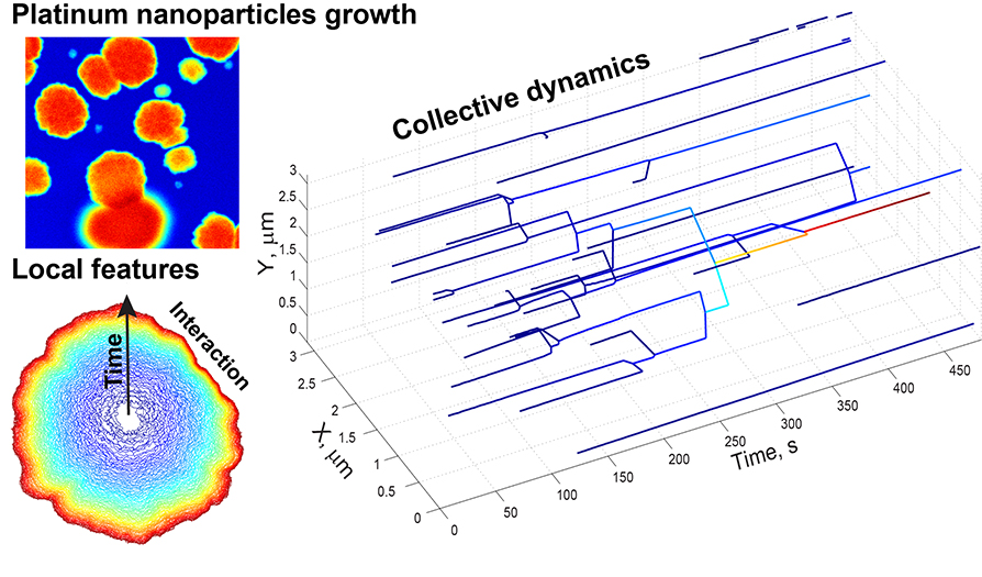
February 4, 2016 – To tailor tiny nanocrystals for catalysts, semiconductors and other applications, scientists must predict what happens inside the particle, at the boundary and in the solvent during particle growth. Researchers at Oak Ridge National Laboratory and the University of Kentucky tackled this tricky task by developing a framework to analyze crystal growth mechanisms, collective dynamics and proximity effects. In situ liquid scanning transmission electron microscopy captured behavior that simulations correlated to physical and chemical phenomena. “Insight into the physics and chemistry of nanocrystals’ formation and growth will improve our understanding of their physiochemical properties,” said postdoctoral fellow Anton Ievlev of the Center for Nanophase Materials Sciences, a Department of Energy User Facility at ORNL. “This knowledge may aid in the design of new materials for microelectronics, biomedicine and other fields.”
Researchers developed a framework to learn physical and chemical phenomena defining nanocrystal growth from scanning transmission electron microscopy.
Media Contact
Dawn Levy
, Senior Science Writer and Communications Specialist, Physical Sciences Directorate
, 865.202.9465
|
LEVYD@ORNL.GOV


