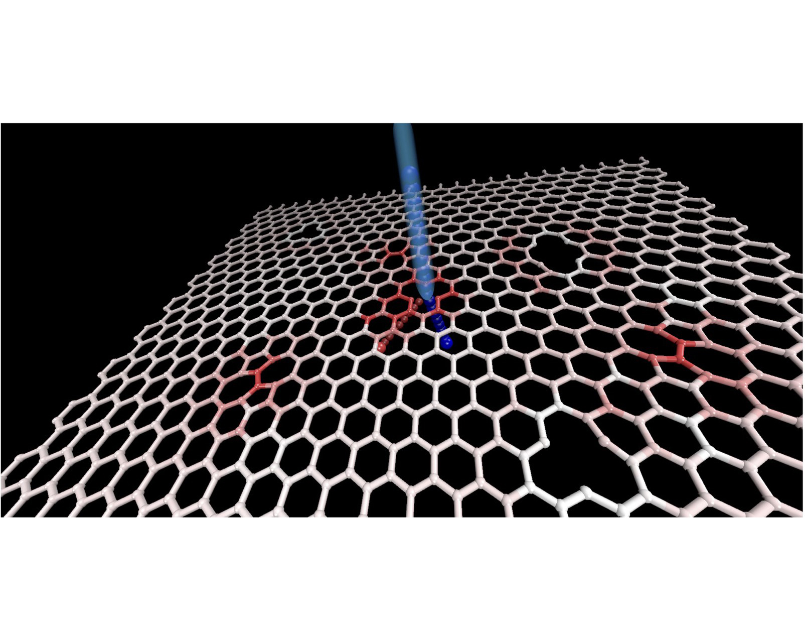
 with a defected graphene sheet and subsequent formation of a carbon vacancy (red). Red shades indicate local strain in the graphene. Image credit: Kichul Yoon, Penn State")
October 7, 2016 – Researchers at Penn State, the Department of Energy’s Oak Ridge National Laboratory and Lockheed Martin Space Systems Company have developed methods to control defects in two-dimensional materials, such as graphene, that may lead to improved membranes for water desalination, energy storage, sensing or advanced protective coatings.
For a two-dimensional, one-atom-thick material like graphene, defects such as small cracks or holes can make a big difference in performance. Usually, these defects are considered undesirable. But if the defects can be controlled, they can be used to engineer new, desirable properties into the material.
“As long as you can control defects, you might be able to synthesize in whatever response the graphene will give you,” says Adri van Duin, corresponding author on a recent paper in the American Chemical Society’s journal ACS Nano. “But that does require that you have very good control over defect structure and defect behavior. What we have done here is a pretty strong step towards that.”
van Duin is the co-inventor and main developer of a mathematical modeling and simulation technique called ReaxFF, which is capable of predicting the interactions of thousands of atoms when they are perturbed by an external force, in this case the bombardment of graphene by atoms of a noble gas.
The noble gases, which include helium, neon, argon, krypton and xenon, are frequently used to create defects in graphene for the purpose of enhancing its properties. By knocking one or more carbon atoms out of graphene’s interlinking hexagons, a structure reminiscent of chicken wire, the resulting hole can be filled by atoms of another material or molecule in a process called doping. Doping can change the chemical or electrical properties of the graphene, to, for example, allow water molecules to flow through while rejecting salt particles.
“We have done a series of atomistic scale simulations where we accelerate noble gas ions into the graphene. The simulations gave much the same defect patterns as experiments,” van Duin says. “That means our simulations can tell experimentalist what dose of atoms at which acceleration they need to get those types of defects.”
Because defects can morph into different shapes or move around in the seconds after creation, his group also simulates putting the graphene in an oven and heating at high temperature, called annealing, to stabilize the structure.
It is unusual for an atomistic simulation to correspond to the same size, time and exposure range as an experiment, due to the computational expense of doing interactions among thousands of atoms over the time scale required to stabilize a material, van Duin says. The reactive force field method (ReaxFF), developed by van Duin and CalTech’s William A. Goddard, is able to model chemical and physical interactions in molecules and materials as bonds between atoms form and break.
Kichul Yoon, the paper’s lead author and a graduate student in van Duin’s group, says, “This study provides insight into the atomistic scale details of graphene irradiation and is a preliminary step in designing functionalized carbon materials in two dimensions.”
van Duin adds, “Clearly there is nothing that makes this exclusive to graphene. Any 2D material can be treated with the same simulations. Anyone who wants to dope a 2D material or understand defects will be interested in these simulations.”
The researchers intend to continue working with Lockheed Martin on aerospace applications and will also pursue the goal of graphene-based water desalination. Jacob Swett of Lockheed Martin prepared the samples used in experiments and was crucial in moving the project forward.
To correlate simulations with experiments, the researchers relied upon the Center for Nanophase Materials Sciences (CNMS), a DOE Office of Science User Facility at ORNL, to create defects using ion bombardment and subsequently characterize those defects using atomic-resolution imaging. “At CNMS, we have state-of-the-art helium and neon ion beam and aberration-corrected scanning transmission electron microscopy instruments that permit atomistic scale characterization,” says Raymond Unocic, a R&D staff scientist at Oak Ridge National Laboratory.
Other contributors to the paper, titled “Atomistic-Scale Simulations of Defect Formation in Graphene Under Noble Gas Ion Irradiation,” were Ali Rahnamoun, a Ph.D. student in van Duin’s group, and Vighter Iberi, David Cullen, Ivan Vlassiouk, Alex Belianinov, Stephen Jesse, Xiahan Sang, Olga Ovchinnikova and Adam Rondinone, all of Oak Ridge National Laboratory, who contributed to the experimental modification and characterization of graphene.
Support was provided as part of the Fluid Interface Reactions, Structures and Transport (FIRST) Center, an Energy Frontier Research Center led by Oak Ridge National Laboratory and funded by the U.S. Department of Energy’s Office of Science.
Adri van Duin is Kenneth Kuan-Yuo Kuo Early Career Professor and professor of mechanical engineering and chemical engineering at Penn State, and director of the Materials Computation Center, a part of the user facilities of the Materials Research Institute. Contact him at acv13@psu.edu.
UT-Battelle manages ORNL for the DOE’s Office of Science. The Office of Science is the single largest supporter of basic research in the physical sciences in the United States, and is working to address some of the most pressing challenges of our time. For more information, please visit http://energy.gov/science/. – by Walt Mills, Penn State
