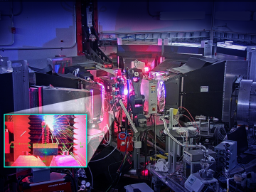
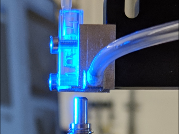
Using neutrons to see the additive manufacturing process at the atomic level, scientists have shown that they can measure strain in a material as it evolves and track how atoms move in response to stress.
Using neutrons to see the additive manufacturing process at the atomic level, scientists have shown that they can measure strain in a material as it evolves and track how atoms move in response to stress.
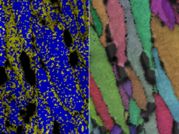
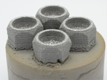
ORNL researchers have identified a mechanism in a 3D-printed alloy – termed “load shuffling” — that could enable the design of better-performing lightweight materials for vehicles.
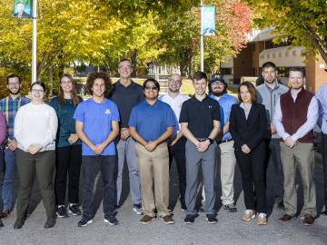
Nine student physicists and engineers from the #1-ranked Nuclear Engineering and Radiological Sciences Program at the University of Michigan, or UM, attended a scintillation detector workshop at Oak Ridge National Laboratory Oct. 10-13.
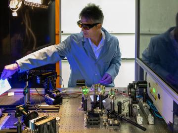
A multidisciplinary team of scientists at ORNL has applied a laser-interference structuring, or LIS, technique that makes significant strides toward eliminating the need for hazardous chemicals in corrosion protection for vehicles.

Six ORNL scientists have been elected as fellows to the American Association for the Advancement of Science, or AAAS.
Researchers at the Department of Energy’s Oak Ridge National Laboratory have received five 2019 R&D 100 Awards, increasing the lab’s total to 221 since the award’s inception in 1963.
Using additive manufacturing, scientists experimenting with tungsten at Oak Ridge National Laboratory hope to unlock new potential of the high-performance heat-transferring material used to protect components from the plasma inside a fusion reactor.
In the shifting landscape of global manufacturing, American ingenuity is once again giving U.S companies an edge with radical productivity improvements as a result of advanced materials and robotic systems developed at the Department of Energy’s Manufac
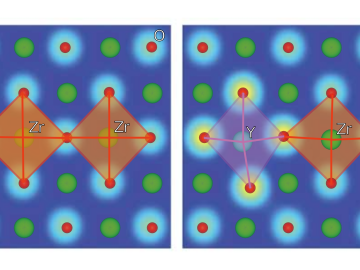
Ionic conduction involves the movement of ions from one location to another inside a material. The ions travel through point defects, which are irregularities in the otherwise consistent arrangement of atoms known as the crystal lattice.

A new method to produce large, monolayer single-crystal-like graphene films more than a foot long relies on harnessing a “survival of the fittest” competition among crystals.