Explore
Find the information, people and opportunities you’re looking for.
Our Strategy: Accelerate innovation
Ensuring U.S. leadership in the development, manufacture, and
deployment of materials, chemistries, and components for energy and security applications.
Biotechnology
Leading the biotechnology revolution to ensure American energy, food security, global competitiveness, and human health.
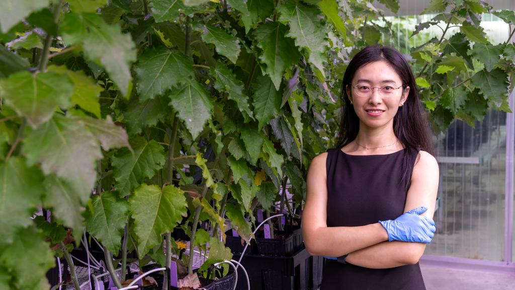
Mengjun Shu: Mapping tree resilience with AI, biological data

Center for Bioenergy Innovation strengthens leadership with new team leads

Samuels receives Health Physics Society’s Elda E. Anderson Award
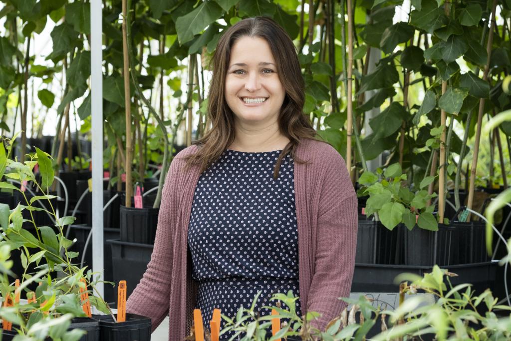
Q&A with Melissa Cregger: From field to factory with precision crops
Materials
Discovering and designing the materials that power U.S. energy, national security, and economic competitiveness.

Department of Energy selects ORNL to lead nine Genesis Mission projects
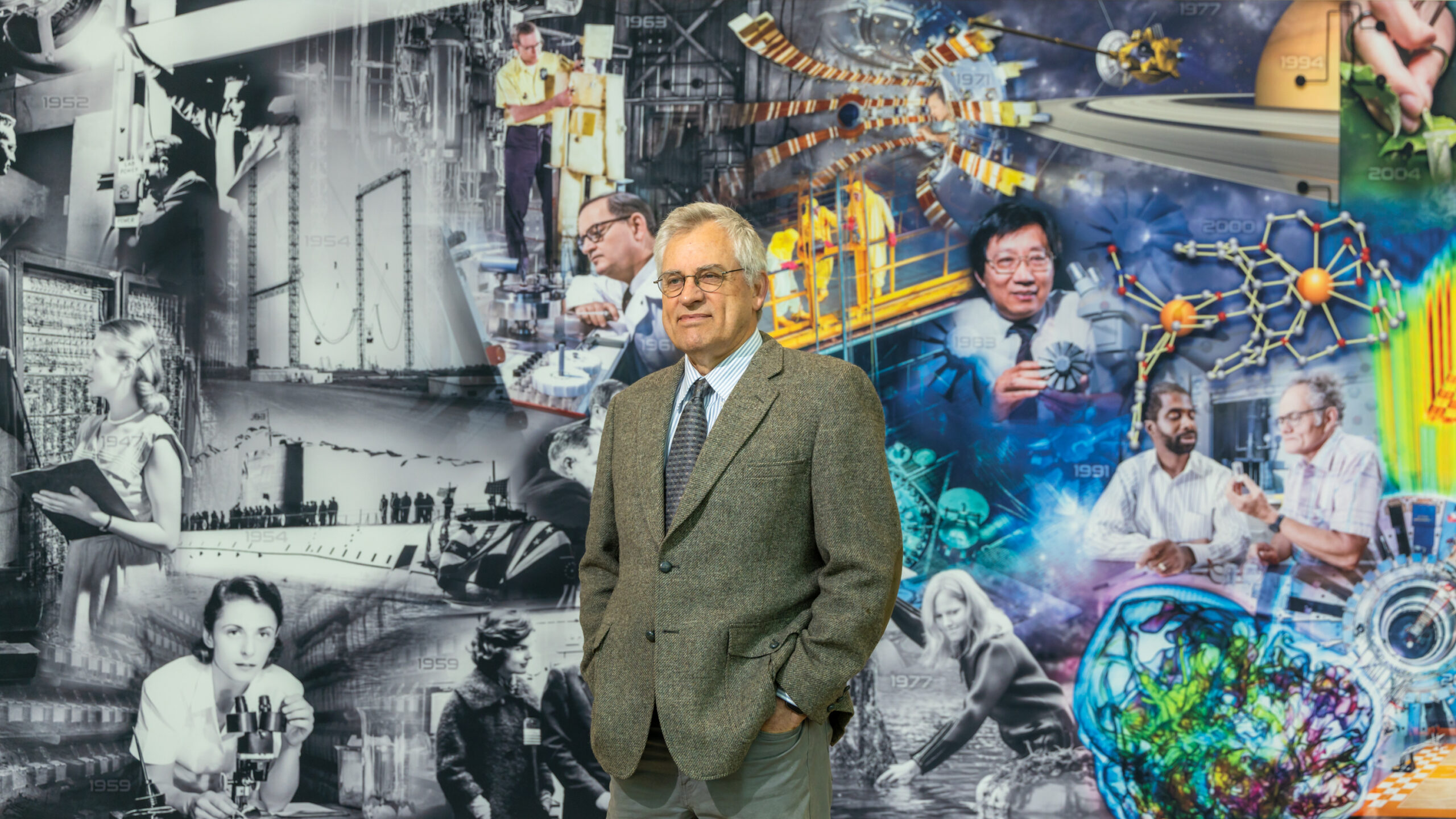
ORNL’s David Radford builds tools to explore deep questions
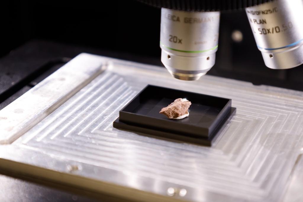
New mineral named for ORNL researcher Tyler Spano
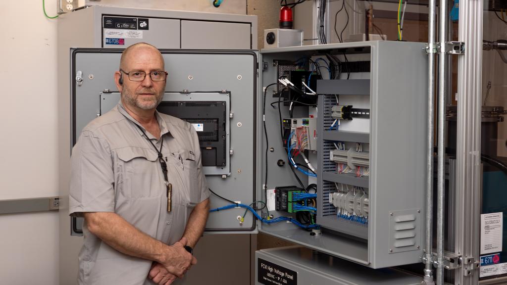
Operations workforce powers ORNL’s autonomous science future
Neutrons
Using world-leading neutron science to reveal the structure and behavior of materials.
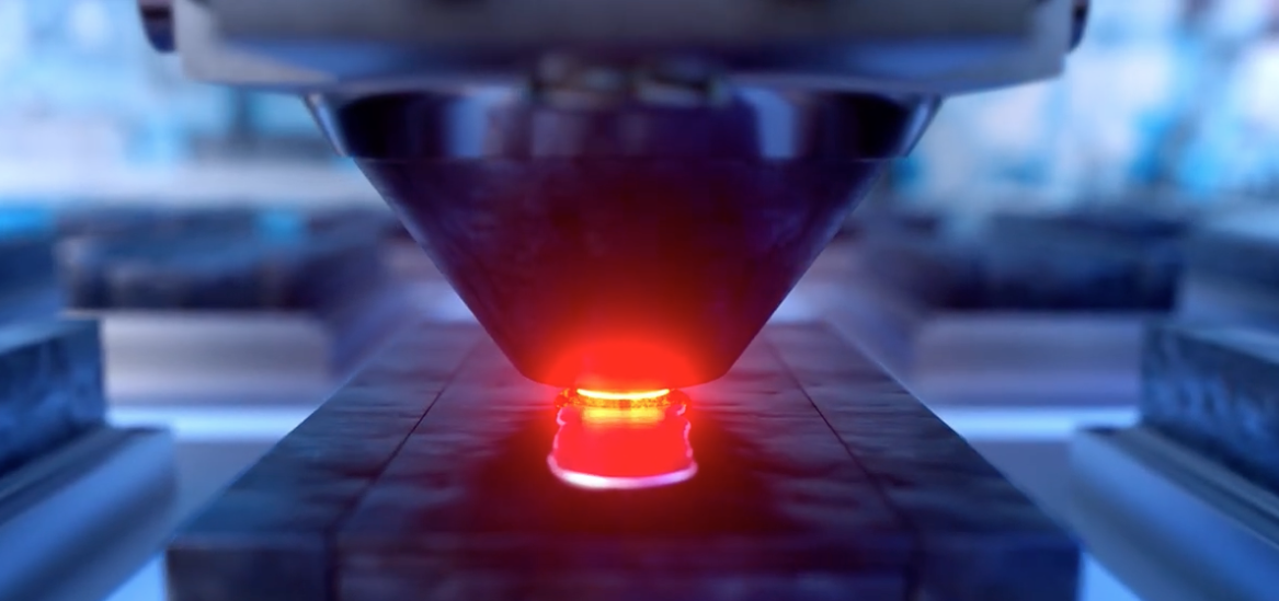
Neutrons reveal how friction stir welding could strengthen steel
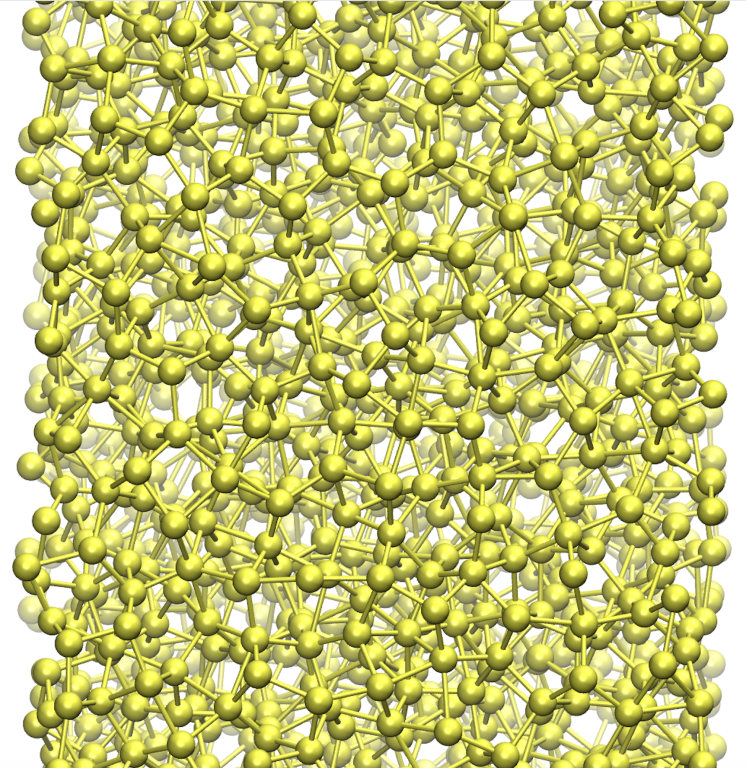
ORNL scientists pinpoint new ways to synthesize power source
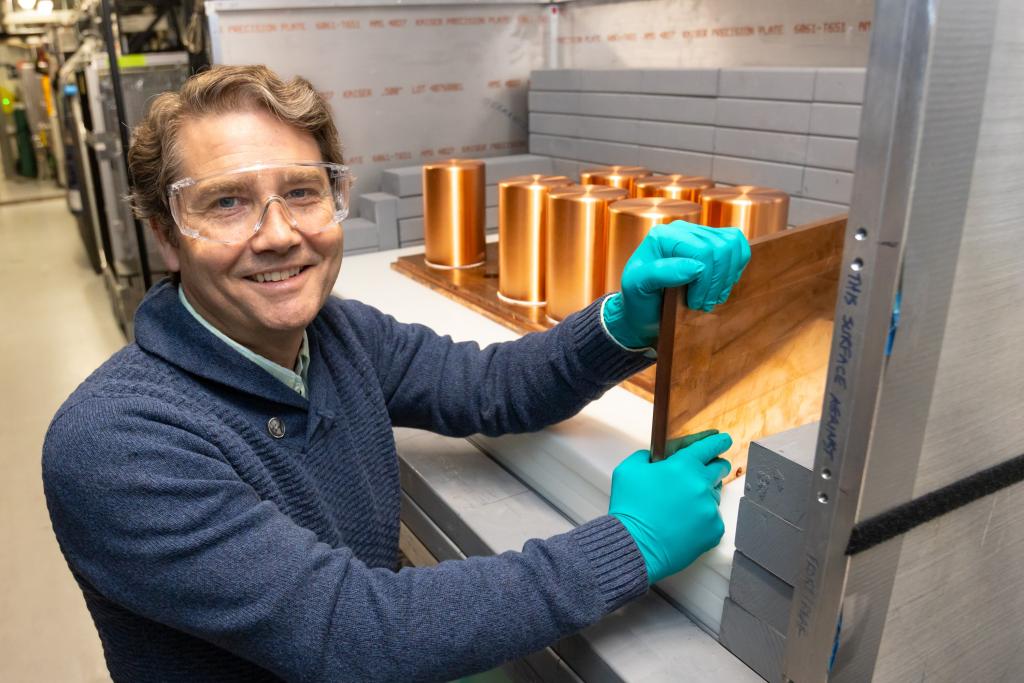
ORNL’s Jason Newby advances neutrino research frontiers

ORNL researchers showcase AI-driven science at national expo
Manufacturing
Integrating advanced materials, artificial intelligence, and digital engineering to strengthen U.S. competitiveness, energy security, and national defense.
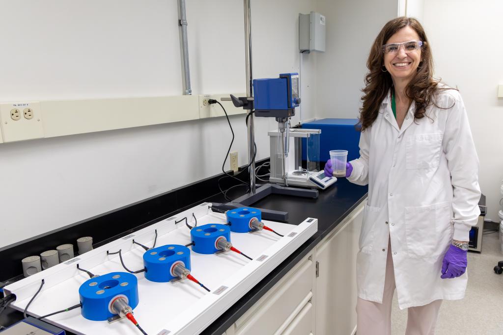
ORNL launches national cement and concrete innovation hub
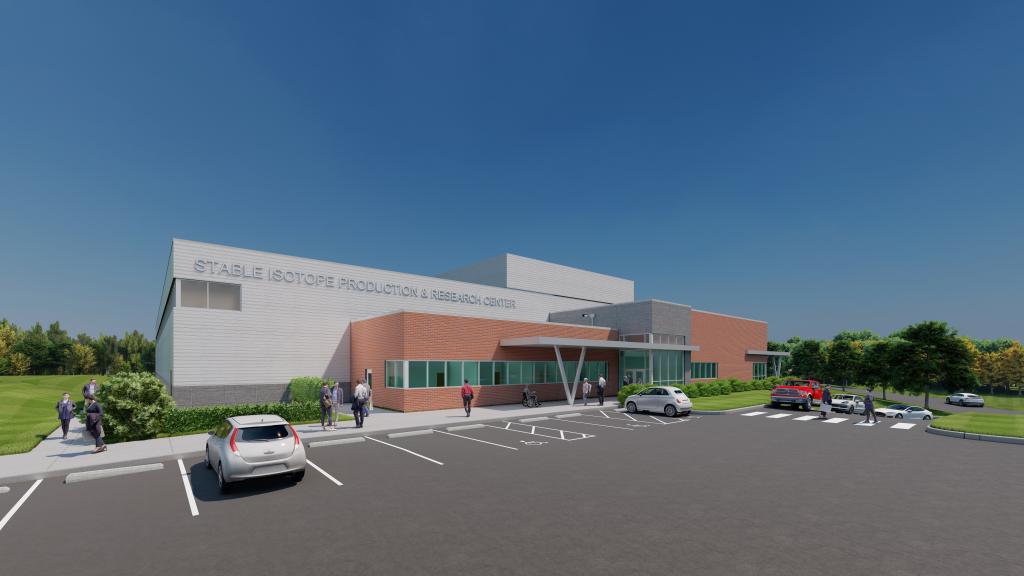
DOE expands stable isotope production capabilities at ORNL

Hassen named Fellow of the American Society for Nondestructive Testing
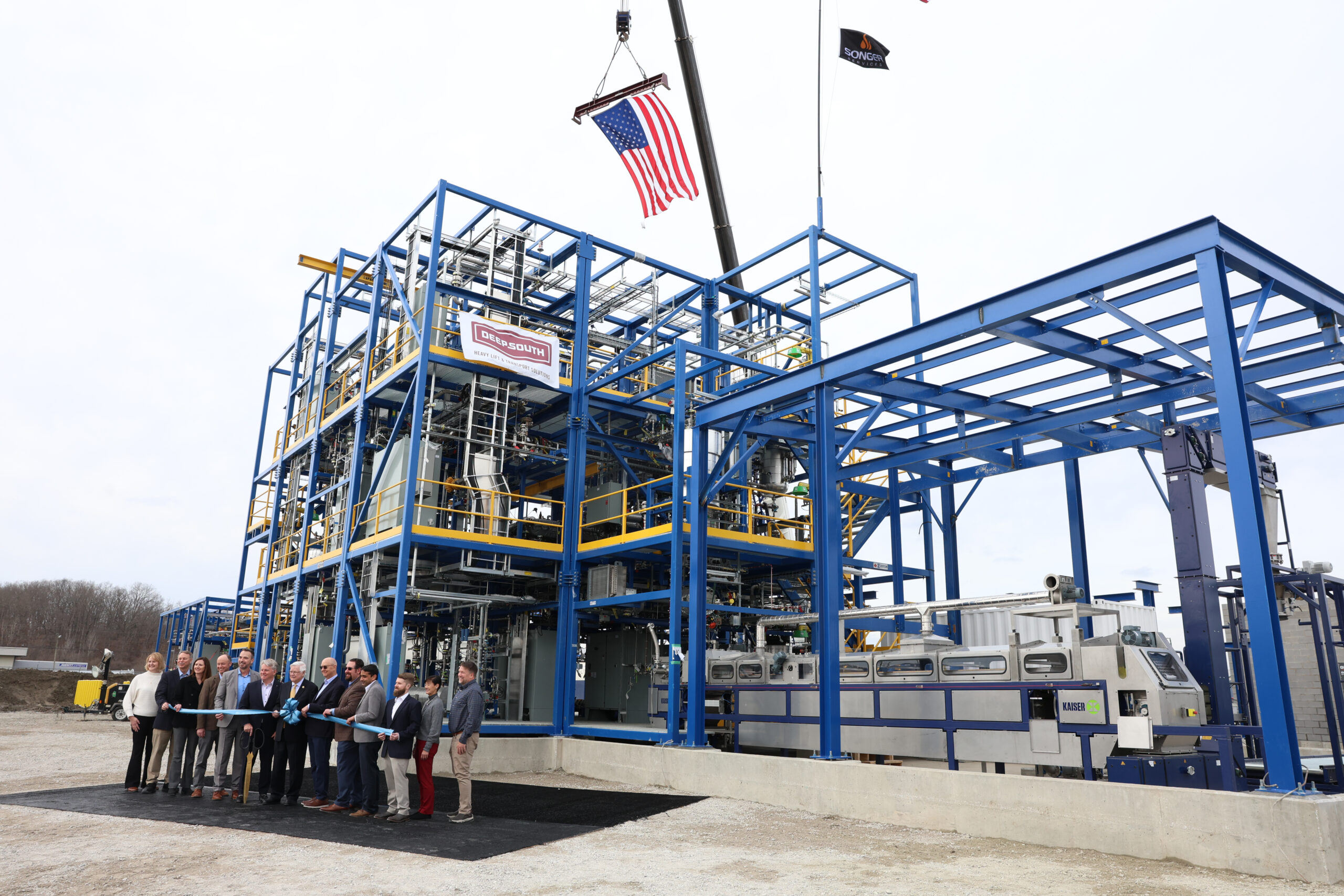
ORNL earns five DOE Transportation Technologies Office awards
Our Strategy: Integration
Creating a smart, post-exascale ecosystem that
integrates HPC, AI, and quantum for open science and national security.
SI
Applying SI to accelerate discovery, strengthen security, and transform complex systems.
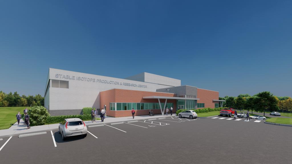
DOE expands stable isotope production capabilities at Oak Ridge National Laboratory
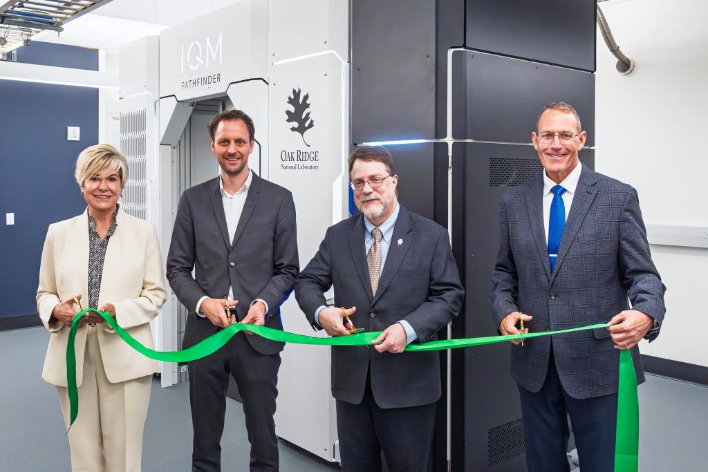
ORNL deploys new IQM quantum computer
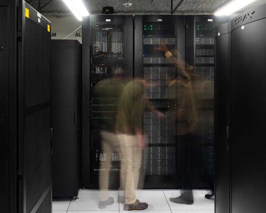
Streamlining ARM data access with AI-ready infrastructure
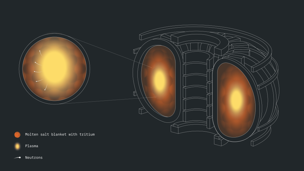
ORNL and partners achieve first-known computations of fusion materials on a quantum computer
Autonomous Science
Combining AI, automation and advanced scientific tools to help researchers accelerate discovery.
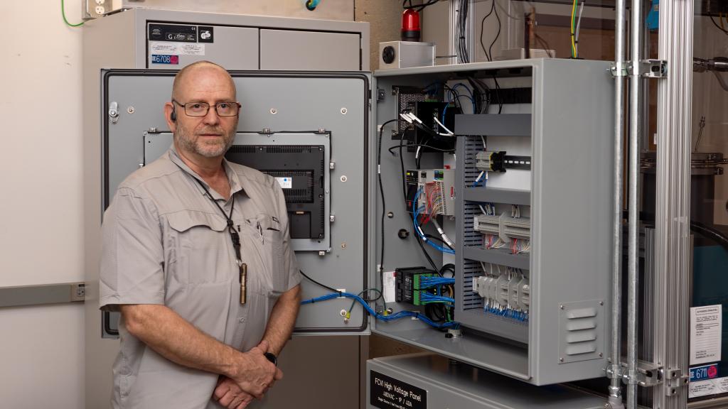
Operations workforce powers ORNL’s autonomous science future
Q&A with Melissa Cregger: From field to factory with precision crops
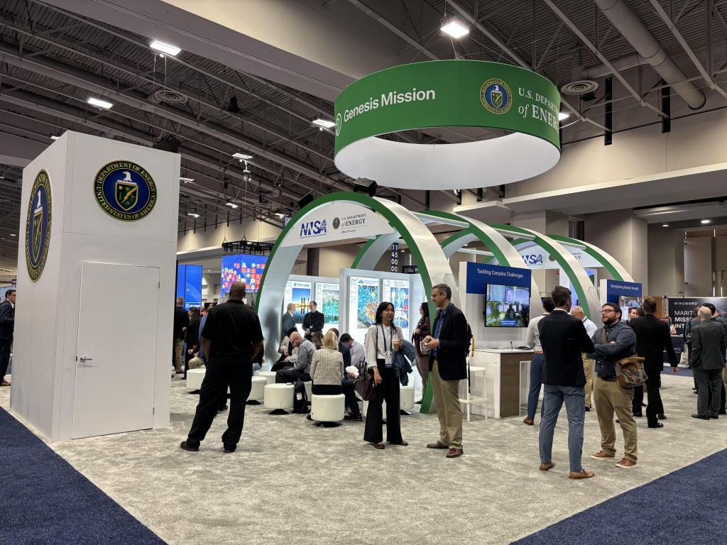
ORNL researchers showcase AI-driven science at national expo
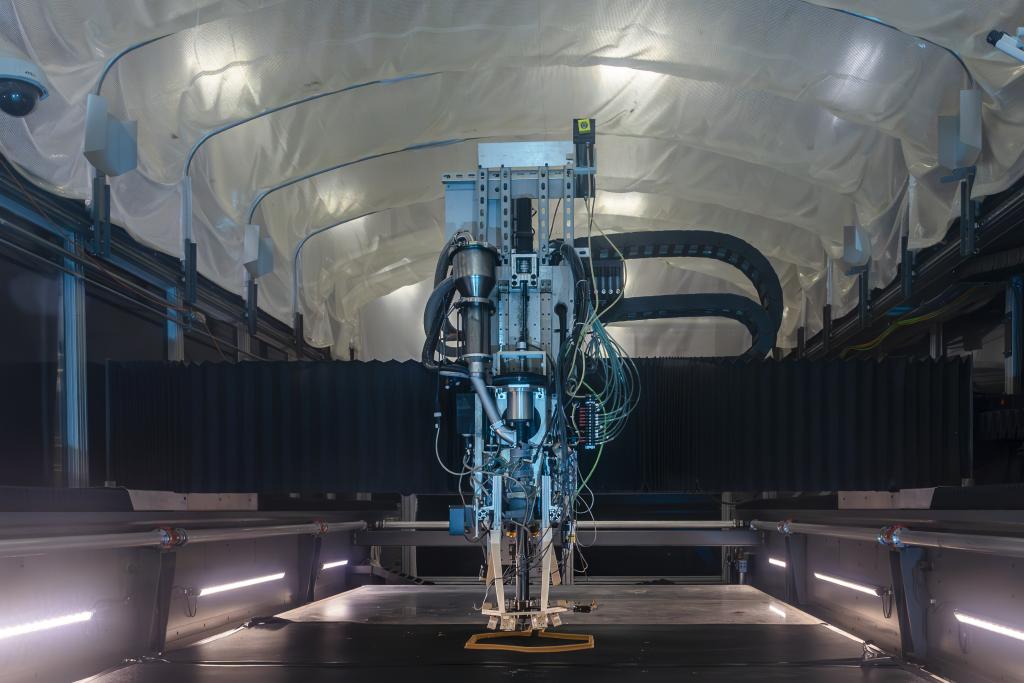
Error correction tech boosts the 3D printing of big composite parts
Quantum
Advancing quantum science to unlock new capabilities in computing, sensing, and secure communication.
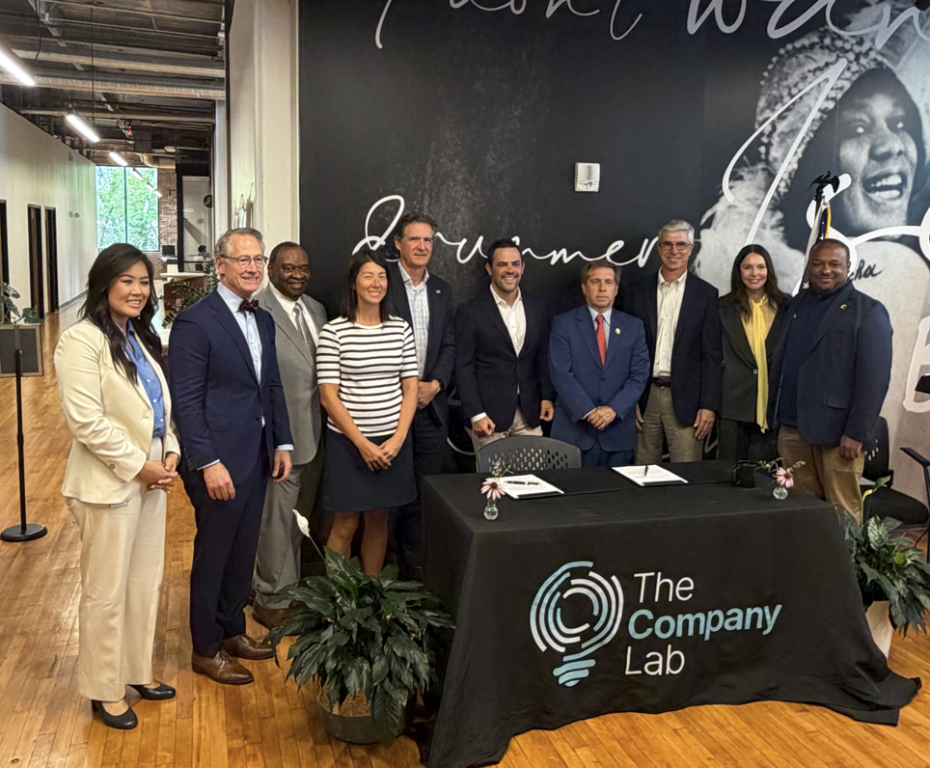
ORNL, Chattanooga startup accelerator partner to expand technology commercialization
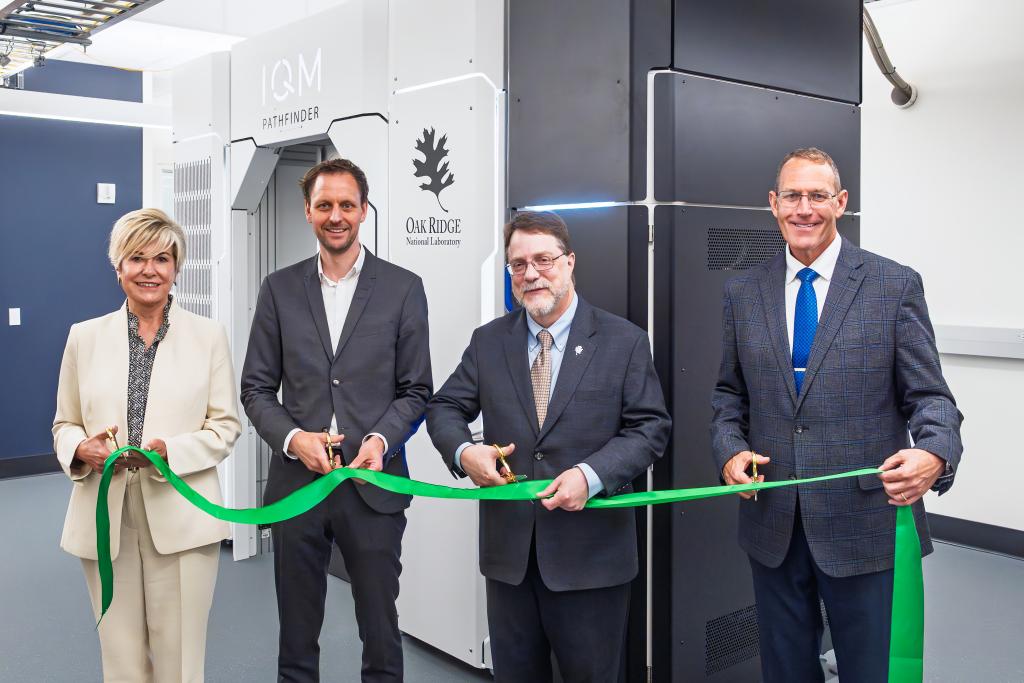
ORNL deploys new IQM quantum computer

Calculating a new view on quantum mechanics using quantum computers
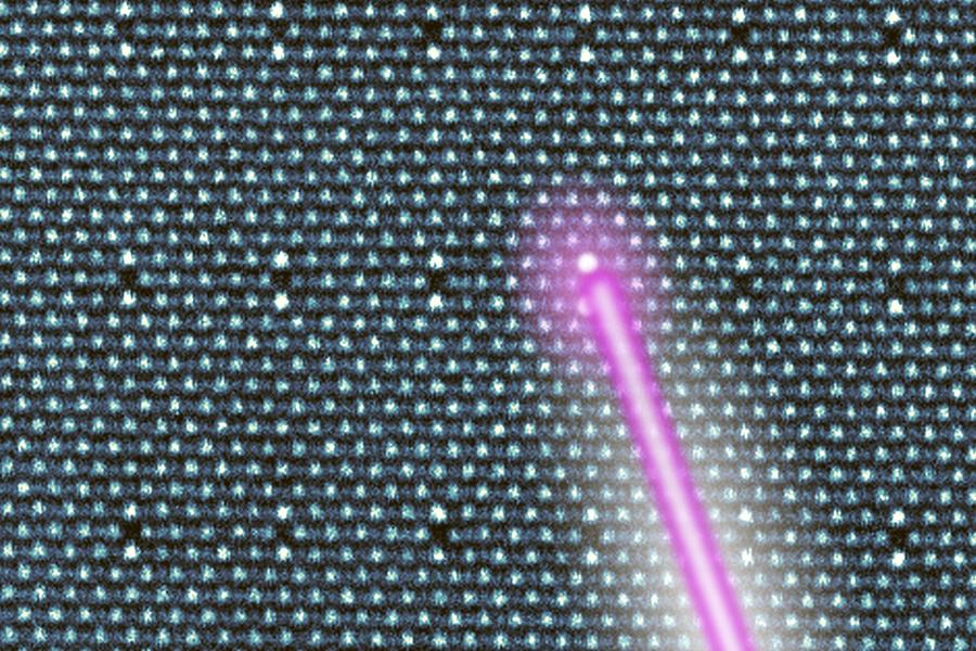
Researchers ‘reprogram’ materials by quickly rearranging their atoms
Our Strategy: De-risk Deployment
Reducing the financial and technical risks of
fission and fusion demonstration and deployment through innovation.
Isotopes
Advancing isotope science for a healthy, secure and reliable future.
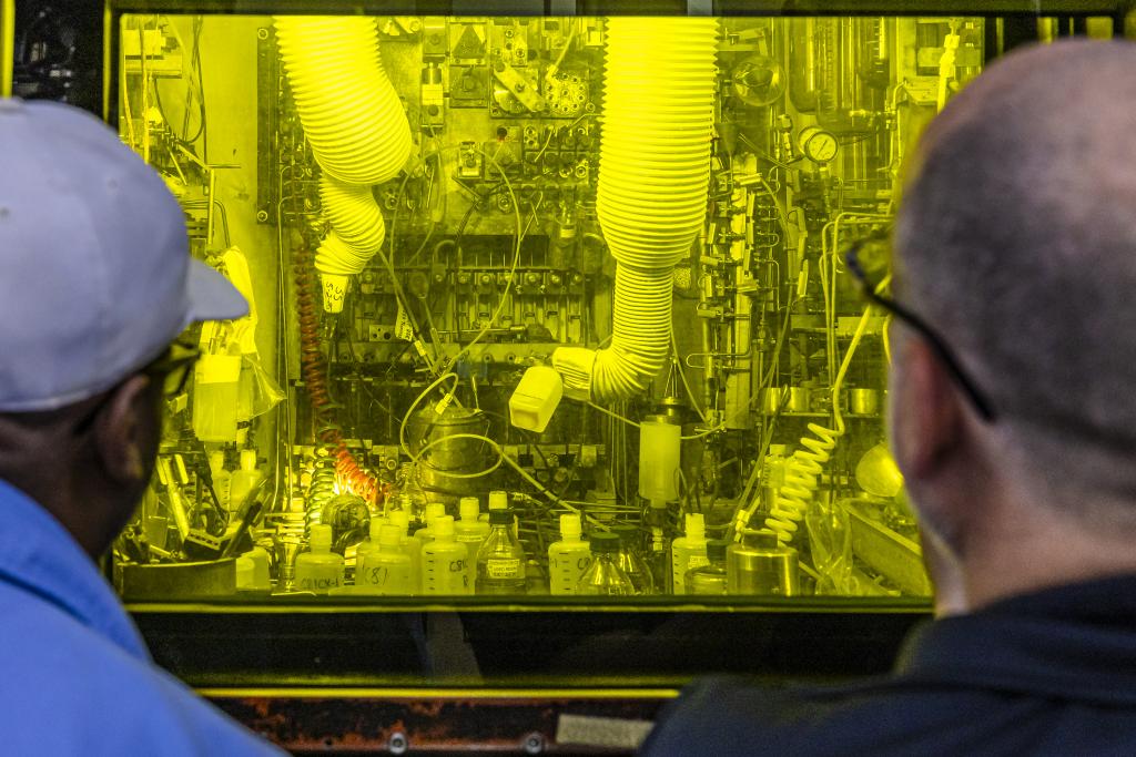
As californium-252 demand climbs, ORNL is increasing production

World-renowned radiopharmaceutical scientist to advance cancer therapies
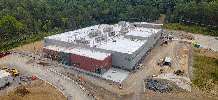
DOE unveils breakthrough in domestic isotope supply chains
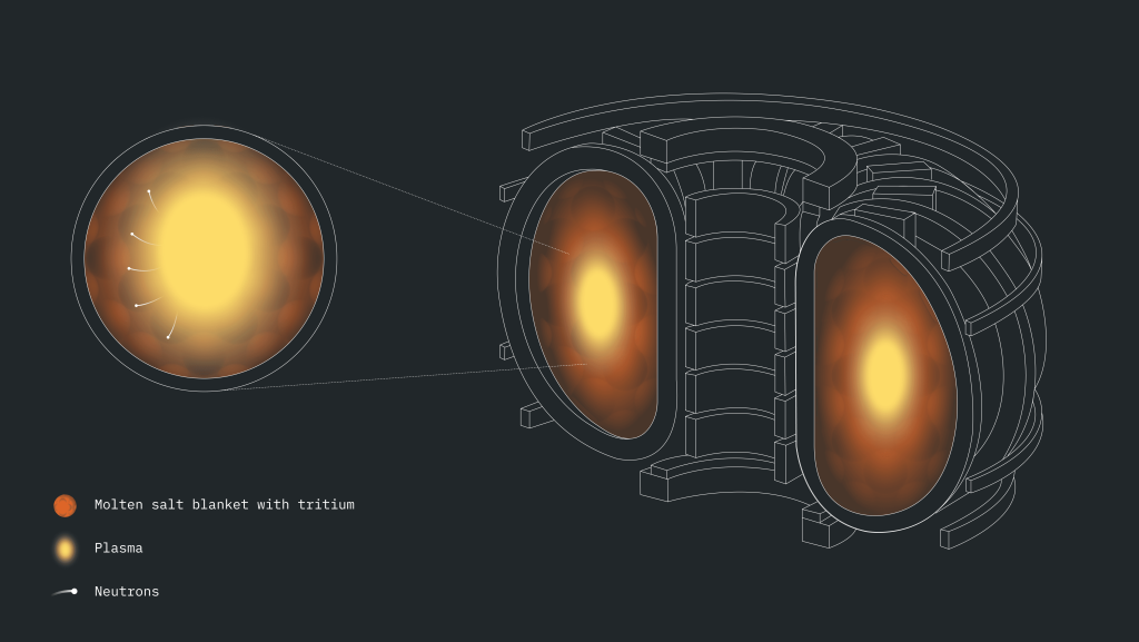
First-known computations of fusion materials on a quantum computer
Fission
Advancing fission to strengthen America’s energy, security, and competitiveness.
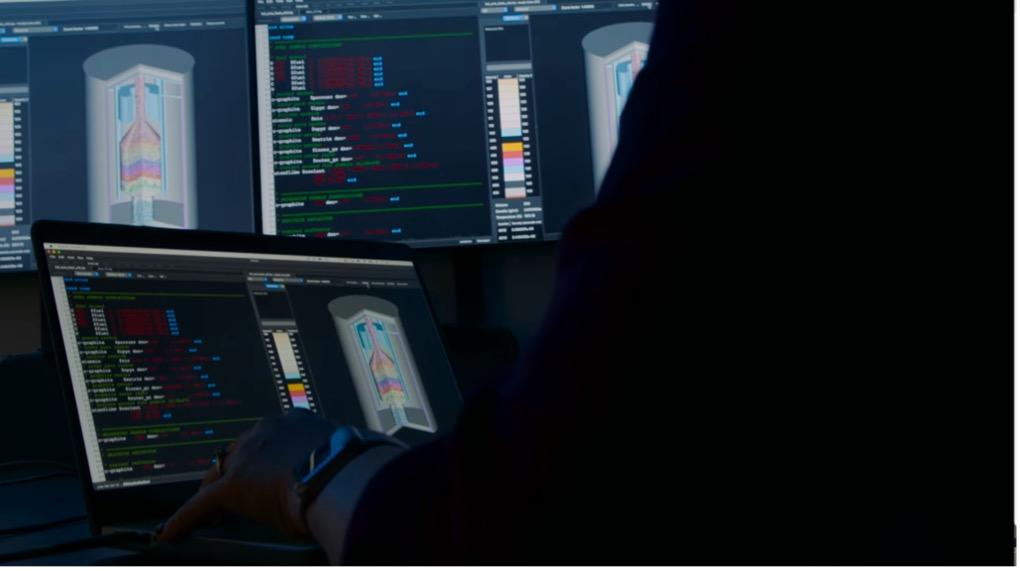
Advanced modeling accelerates nuclear energy
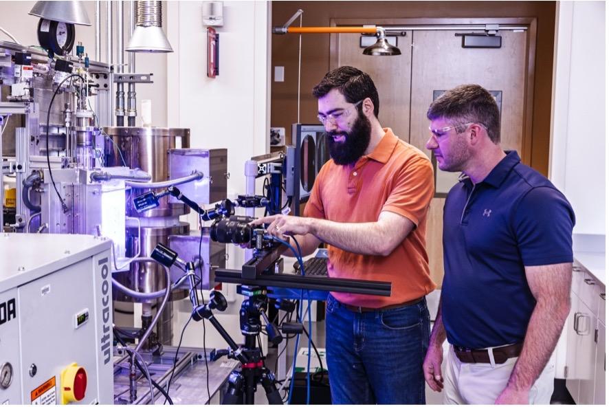
Fast-tracking efficiency in light water reactor fuels
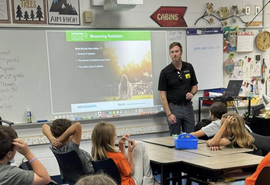
Small core, big energy: ORNL-led Nuclear Day engages students in STEM
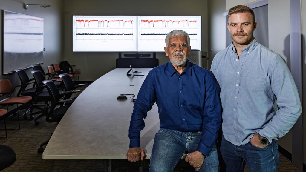
A powerful pairing introduces new method of non-destructive testing
Fusion
Harnessing the power of the stars to make commercial fusion energy a reality.
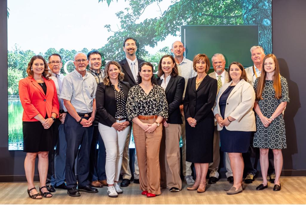
ORNL, REV launch innovative collaboration on fusion infrastructure

New Innovation Crossroads cohort tackles DOE’s toughest challenges
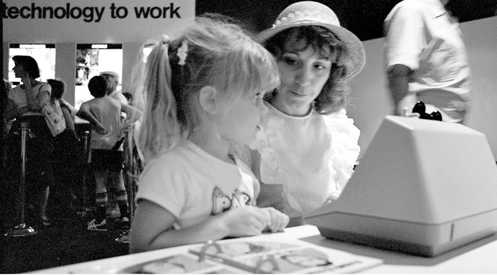
Prolific patenting: Sam Hurst’s legacy of invention at ORNL
Small core, big energy: ORNL-led Nuclear Day engages students in STEM
Our Strategy: Modernization

Powering resilient, affordable and secure energy systems for America.
Buildings
Building technologies for reliable and affordable energy

Wagner awarded ASME’s 2026 Henry Laurence Gantt Medal

ORNL to feature transformative tech at ARPA-E summit
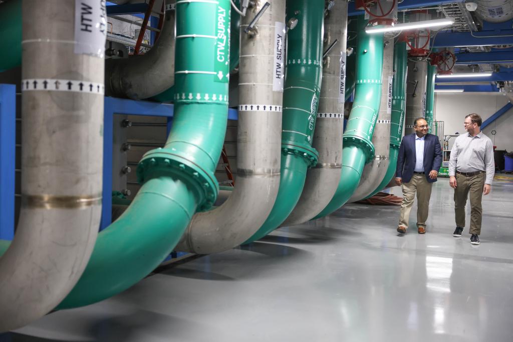
Oak Ridge National Laboratory launches the Next-Generation Data Centers Institute
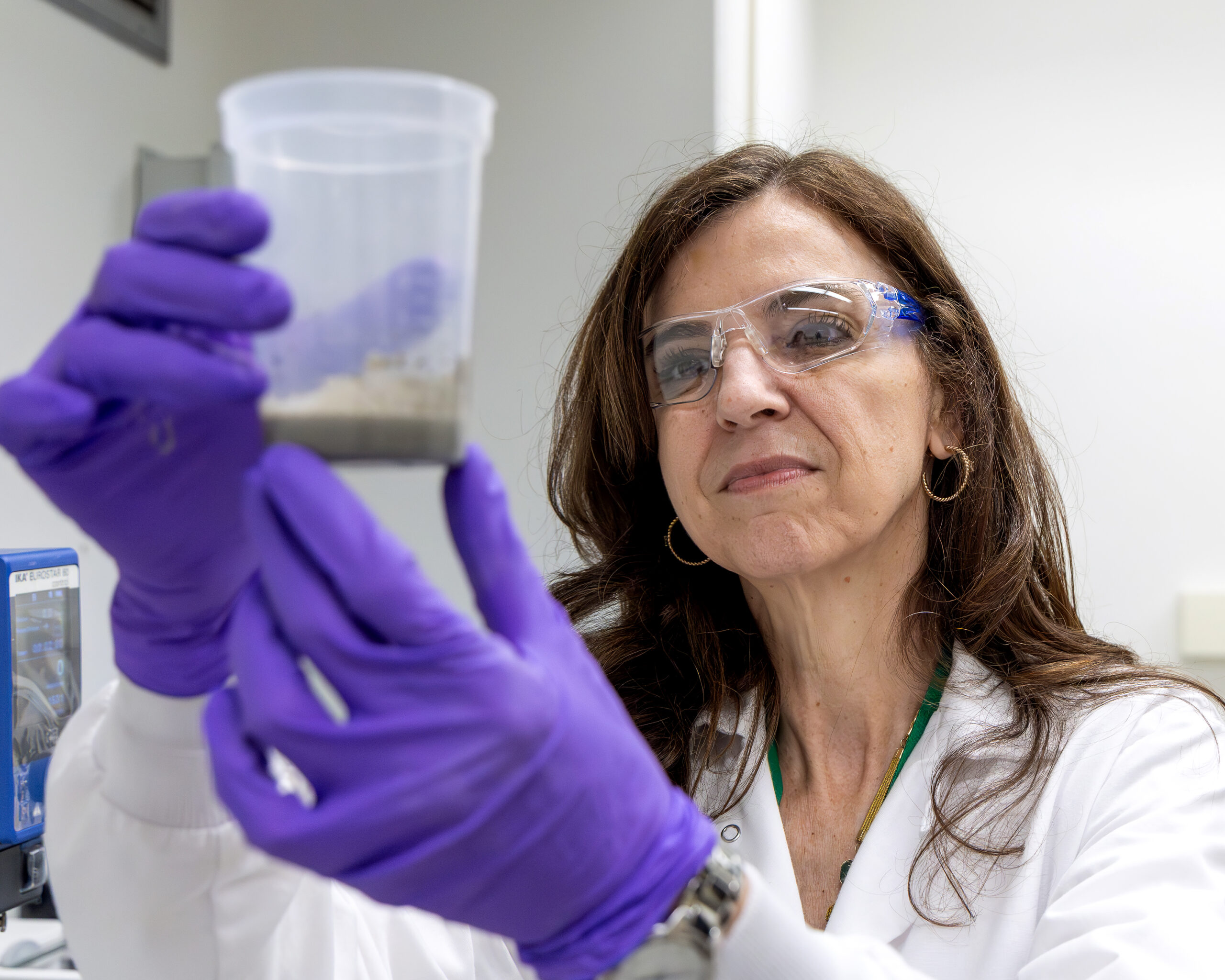
Silva named a Fellow of the American Ceramic Society
Grid
Building a smarter, stronger U.S. electric grid
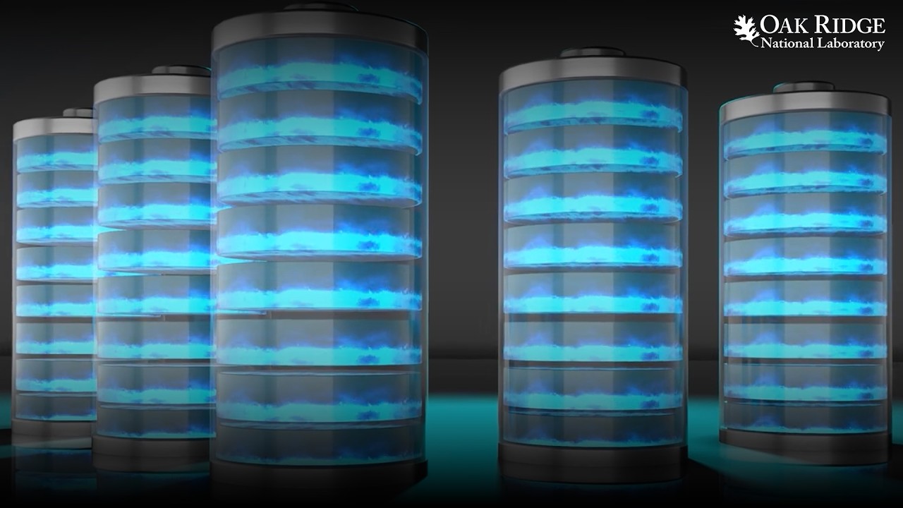
Modeling framework reveals grid battery aging effects

Wagner awarded ASME’s 2026 Henry Laurence Gantt Medal
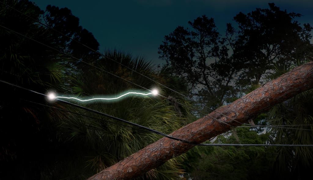
New AI-enhanced tools detect electrical arcing, reduce wildfires
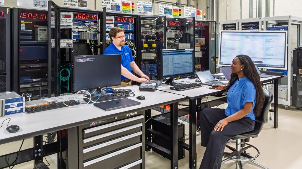
ORNL-developed cybersecurity framework graduates from lab to electric grid
Regional resilience
Uniting science and expertise to strengthen energy resilience and economic security.
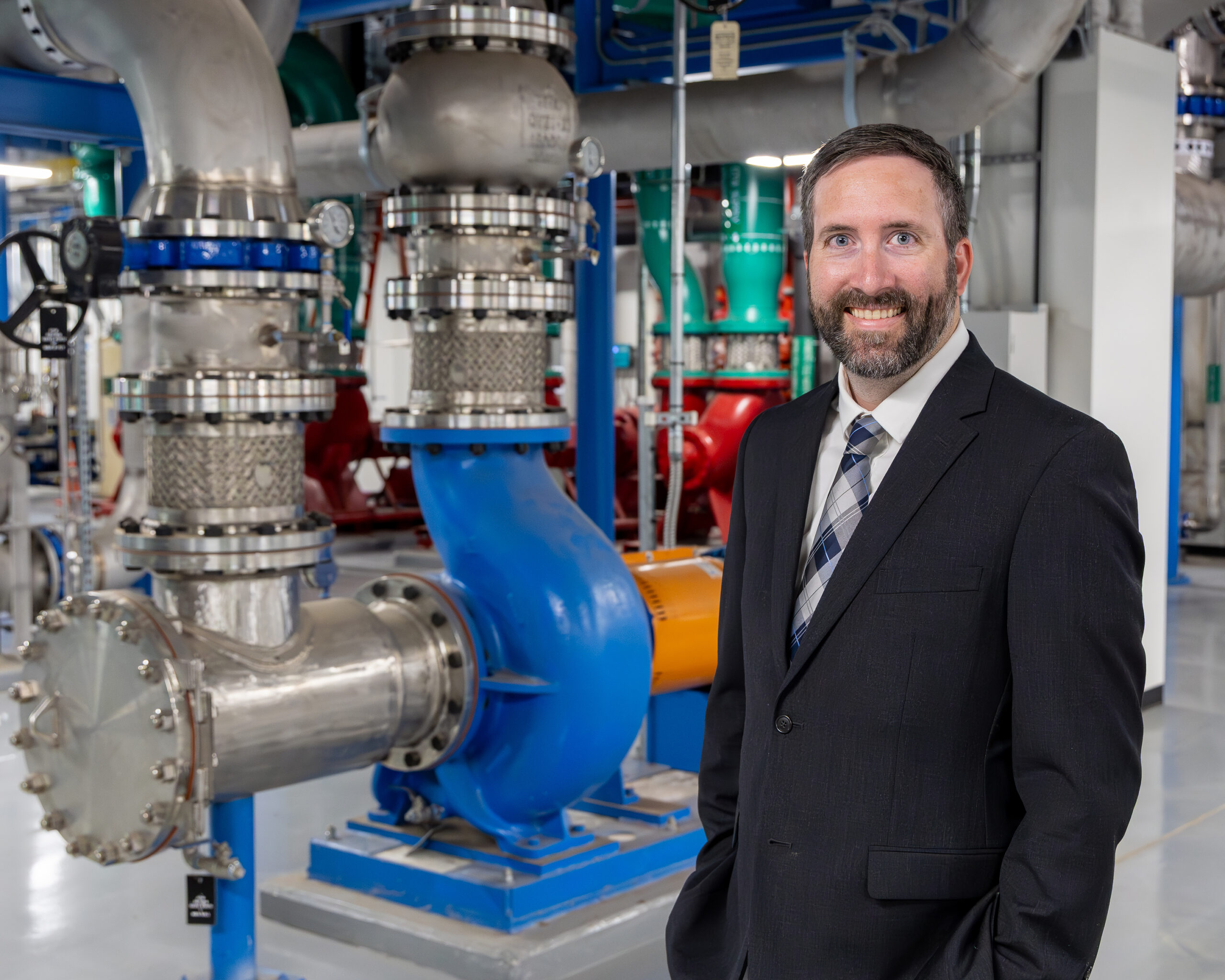
Tapping water supply systems for energy production
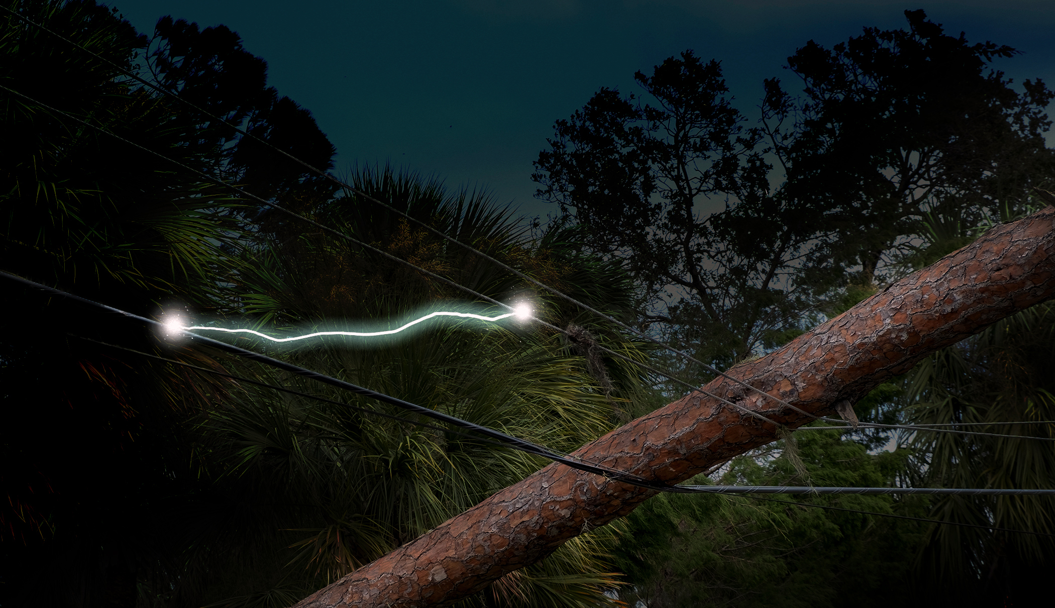
New AI-enhanced tools detect electrical arcing, reduce wildfires

What 100,000 simulations reveal about our power grid
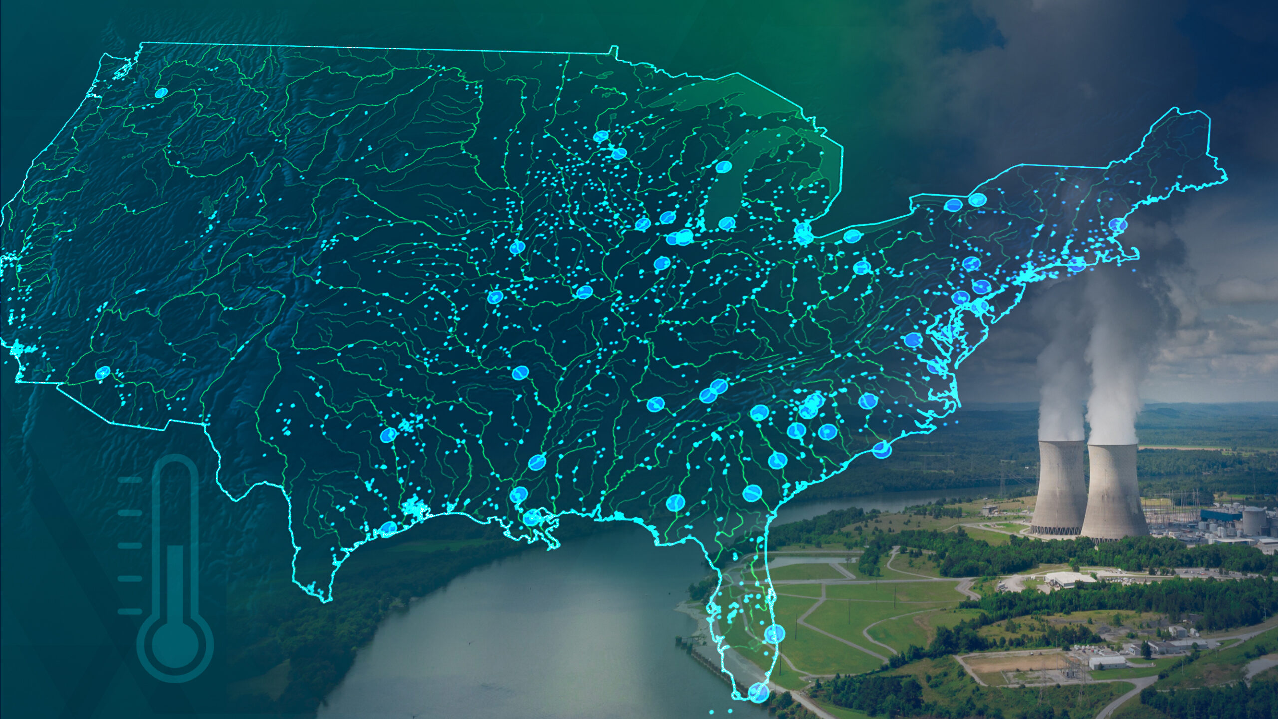
AI model delivers river temperature insights, strengthening US energy security
Transportation
Strengthening the technologies and systems that move people, goods and energy across the nation.
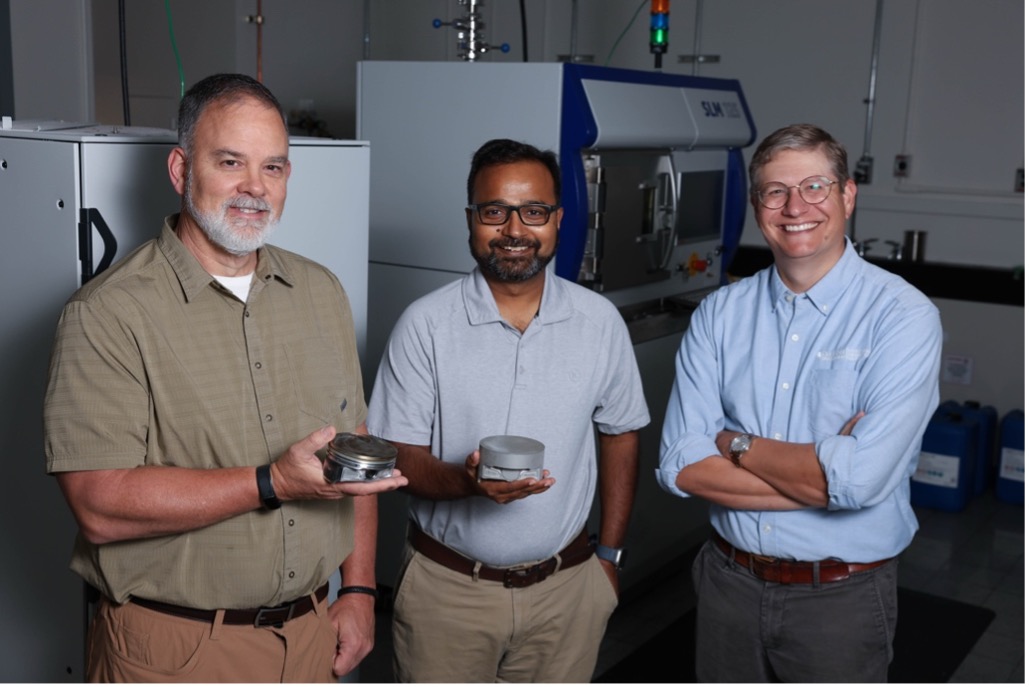
Novel high-temperature alloys enable lighter, more fuel-efficient truck engines
ORNL partnership helps ACP Technologies scale materials for graphite and carbon fiber

ORNL earns five DOE Transportation Technologies Office awards

New motor drive design reduces heat, wear in high-power systems
ORNL Overview
Discover the mission, history, leadership and values that guide ORNL’s work.
Operations
Explore how operational excellence guides the way we plan, perform and improve our work at ORNL as we take on some of the nation’s most important scientific and technical challenges.
Partnerships
Find the partnership opportunities, expertise and capabilities to help move your ideas forward.