Scientific Achievement
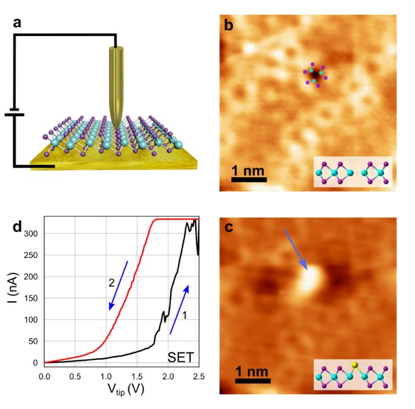
The first direct observation of non-volatile resistive switching (NVRS) phenomenon via metal ion migration to and from single vacancy sites on monolayer MoS2.
Significance and Impact
Work shows a new avenue for application of atomic-scale memory devices, enabling substantial advances in high-density data storage, neuromorphic computing, and radio-frequency reconfigurable communication systems.
Research Details
– Scanning tunneling microscopy (STM) is used as an atomic-scale imaging, manipulation, spectroscopy, and transport measurement tool to observe the NVRS switching.
– STM results are corroborated by computational studies of defect structures and electronic states.
Saban M. Hus, Ruijing Ge, Po-An Chen, Liangbo Liang, Gavin E. Donnelly, Wonhee Ko, Fumin Huang, Meng-Hsueh Chiang, An-Ping Li, and Deji Akinwande, “Observation of Single-defect Memristor in an MoS2 Atomic Sheet,” Nature Nanotechnology (2020). DOI: 10.1038/s41565-020-00789-w