electron Microscopy and Microanalysis Group
The electron Microscopy and Microanalysis (eMMA) group’s mission is to "understand materials’ structure, chemistry, and function through the development and application of advanced analytical microscopy, atom probe tomography, and cryo-electron microscopy techniques."
The eMMA group at the Center for Nanophase Materials Sciences (CNMS) is dedicated to pioneering advanced, multi-scale materials characterization techniques that are aimed at uncovering vital structure-property-function correlations for materials research.
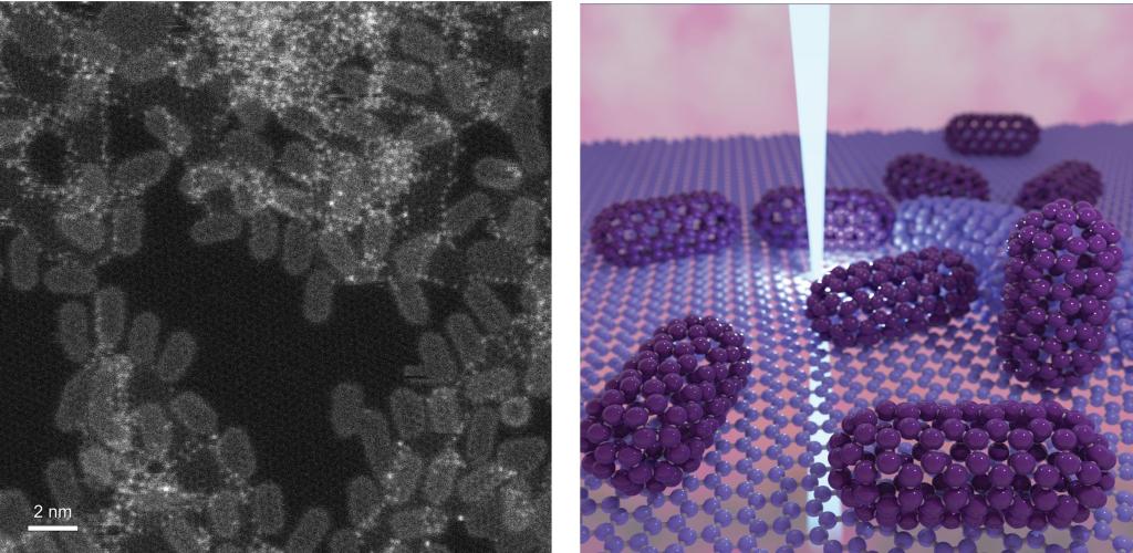
Our group specializes in the development and application of aberration-corrected STEM imaging, spectroscopy (electron energy loss spectroscopy and energy dispersive), and electron diffraction methods for a wide range of materials (metals/alloys, ceramics, composites, biological, and nanomaterials) used in energy storage, catalysis, quantum, structural, nuclear, biopreparedness, and theranostic applications. Our microscopes are uniquely equipped for in situ/operando microscopy experimentation with specialized holders and systems that allow us to image and analyze materials response under a range of sample of environments (liquid, gas, vacuum) and external stimuli such as temperature, pressure, laser irradiation, and electrical bias. We have a full suite of cryogenic preparation equipment and dedicated, semi-automated cryo-electron microscopes that are used to study biological specimens, macromolecular structures, and beam-sensitive materials at near-atomic resolution.
The group uses the Z-contrast imaging mode to image composition at atomic scale, Lorentz imaging mode to map in-plane magnetic textures and their response to various external stimuli, and high-energy-resolution electron energy loss spectroscopy (EELS) to probe their local vibrational, optical, and electronic responses at variable temperatures. When combined with the theory, computational, and scattering capabilities offered by other groups and the SNS, the state-of-the-art microscopy facilities at the CNMS offer many complementary routes to analyze next-generation materials working up from the atomic scale.
Our atom probe tomography facility (local electrode atom probe and dual beam SEM/FIB for specimen preparation) allows us to study the 3-D chemical composition with sub-nm resolution. Our team benefits from collaboration between DNA and NTI research groups to develop AI/ML-driven workflows to efficiently explore, analyze, and interpret data.