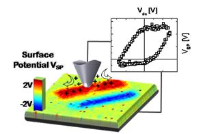
The implementation of contact mode Kelvin probe force microscopy (cKPFM) allows, for the first time, to study bias-induced changes of surface charges at high temporal and lateral resolutions, surpassing traditional non-contact KPFM. Observations of significant surface charge states at zero bias and strong hysteretic electromechanical responses due to dynamic charge trapping and de-trapping at a non-ferroelectric surface have significant implications for fields such as triboelectricity and piezoresponse force microscopy. In the past, electrostatic tip–sample interactions in contact mode were neglected for a variety of scanning probe microscopy–based techniques used to study electromechanical effects. The work presented here emphasizes how important it is to take electrostatic forces into consideration to avoid misinterpretation of experimental data.
N. Balke, P. Maksymovych, S. Jesse, I. I. Kravchenko, Q. Li, and S. V. Kalinin, “Exploring Local Electrostatic Effects with Scanning Probe Microscopy: Implications for Piezoresponse Force Microscopy and Triboelectricity,” ACS Nano (2014). DOI:10.1021/nn505176a
For more information