
An all-in-one experimental platform developed at Oak Ridge National Laboratory’s Center for Nanophase Materials Sciences accelerates research on promising materials for future technologies.
Oak Ridge National Laboratory researchers have built a novel microscope that provides a “chemical lens” for viewing biological systems including cell membranes and biofilms.

Oak Ridge National Laboratory researchers have discovered a better way to separate actinium-227, a rare isotope essential for an FDA-approved cancer treatment.
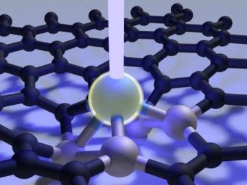
Scientists at Oak Ridge National Laboratory used a focused beam of electrons to stitch platinum-silicon molecules into graphene, marking the first deliberate insertion of artificial molecules into a graphene host matrix.

Liam Collins was drawn to study physics to understand “hidden things” and honed his expertise in microscopy so that he could bring them to light.
![2018-P07635 BL-6 user - Univ of Guelph-6004R_sm[2].jpg](/sites/default/files/styles/list_page_thumbnail/public/2018-P07635%20BL-6%20user%20-%20Univ%20of%20Guelph-6004R_sm%5B2%5D.jpg?itok=DUdZNt_q "2018-P07635 BL-6 user - Univ of Guelph-6004R_sm[2].jpg")
A team of scientists, led by University of Guelph professor John Dutcher, are using neutrons at ORNL’s Spallation Neutron Source to unlock the secrets of natural nanoparticles that could be used to improve medicines.
Physicists turned to the “doubly magic” tin isotope Sn-132, colliding it with a target at Oak Ridge National Laboratory to assess its properties as it lost a neutron to become Sn-131.

An Oak Ridge National Laboratory-led team used a scanning transmission electron microscope to selectively position single atoms below a crystal’s surface for the first time.

Sergei Kalinin of the Department of Energy’s Oak Ridge National Laboratory knows that seeing something is not the same as understanding it. As director of ORNL’s Institute for Functional Imaging of Materials, he convenes experts in microscopy and computing to gain scientific insigh...

An Oak Ridge National Laboratory–led team has learned how to engineer tiny pores embellished with distinct edge structures inside atomically-thin two-dimensional, or 2D, crystals. The 2D crystals are envisioned as stackable building blocks for ultrathin electronics and other advance...