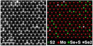
A new
-contrast image analysis method now allows dopant atoms in two-dimensional materials to be located and quantified. With this ability, the distribution of dopants can be verified as the physical and chemical properties are modified. This new capability was used to study doped molybdenum disulfide in which the optical band gap was tuned between 1.85 and 1.60 eV by changing Se concentration. Controlling and quantifying dopant concentration within each atomic layer of 2D ternary compounds provides an efficient method to modify their local properties, and is thus of particular importance for practical applications of 2D materials. The new quantitative
-contrast image analysis method reported in our work1 overcomes the main challenge of quantifying and locating the dopant atoms within each atomic layer, and achieves layer-by-layer mapping of dopants in a bilayer structure for the first time. Our results provide new insights into the growth mechanism and alloying behavior in 2D dichalcogenide atomic layers, and demonstrate that growth of uniform ternary 2D dichalcogenide alloy films with tunable electronic properties is feasible.
Yongji Gong, Zheng Liu, Andrew R. Lupini, Gang Shi, Junhao Lin, Sina Najmaei, Zhong Lin, Ana Laura Elías, Ayse Berkdemir, Ge You, Humberto Terrones, Mauricio Terrones, Robert Vajtai, Sokrates T. Pantelides, Stephen J. Pennycook, Jun Lou, Wu Zhou, Pulickel M. Ajayan, “Band Gap Engineering and Layer-by-Layer Mapping of Selenium-doped Molybdenum Disulfide,” Nano Lett. 14, 442-449 (2014). dx.doi.org/10.1021/nl4032296
For more information